Mechanisms of the performance enhancement by hetero - Gate dielectric in tunnel field - effect transistors
The hetero-gate dielectric (HGD) structure has recently been demonstrated experimentally
in tunnel field-effect transistors (TFETs) to enhance their electrical performance. In this
paper, we adequately examine the mechanisms that the HGD works to ameliorate the
electrical characteristics of TFETs. A typical bulk p-i-n TFET structure is used to exclude
the uncertain effects of body factors on the role of HGD. It is showed that the subthreshold
swing is improved by the presence of a conduction band well near the source/channel
junction, but the swing improvement is limited by the appearance of the hump effect when
the local potential well approaches the source. By analyzing the roles of dielectric
heterojunctions at source- and channel-sides separately, it is found that the on-current
enhanced by the source-side heterojunction is about 5 times larger than by the channel-side
one. The reason is that the source-side heterojunction directly modulates the on-state tunnel
width, whereas the channel-side heterojunction indirectly affects the on-current through
modulating the subthreshold-state tunnel width. Exactly understanding the mechanisms of
the performance enhancement by HGD is important in studying the optimal design of HGDTFETs.
Trang 1
Trang 2
Trang 3
Trang 4
Trang 5
Trang 6
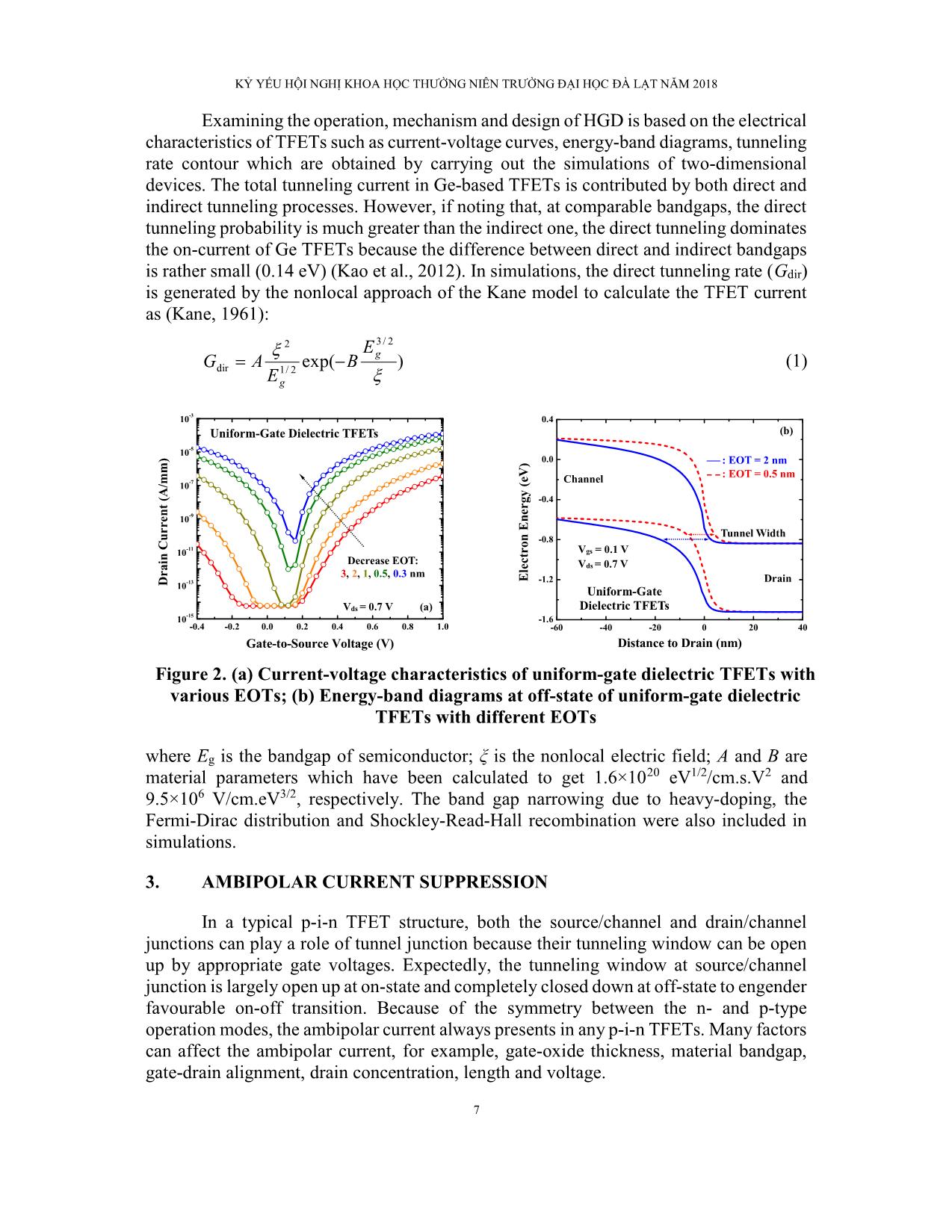
Trang 7
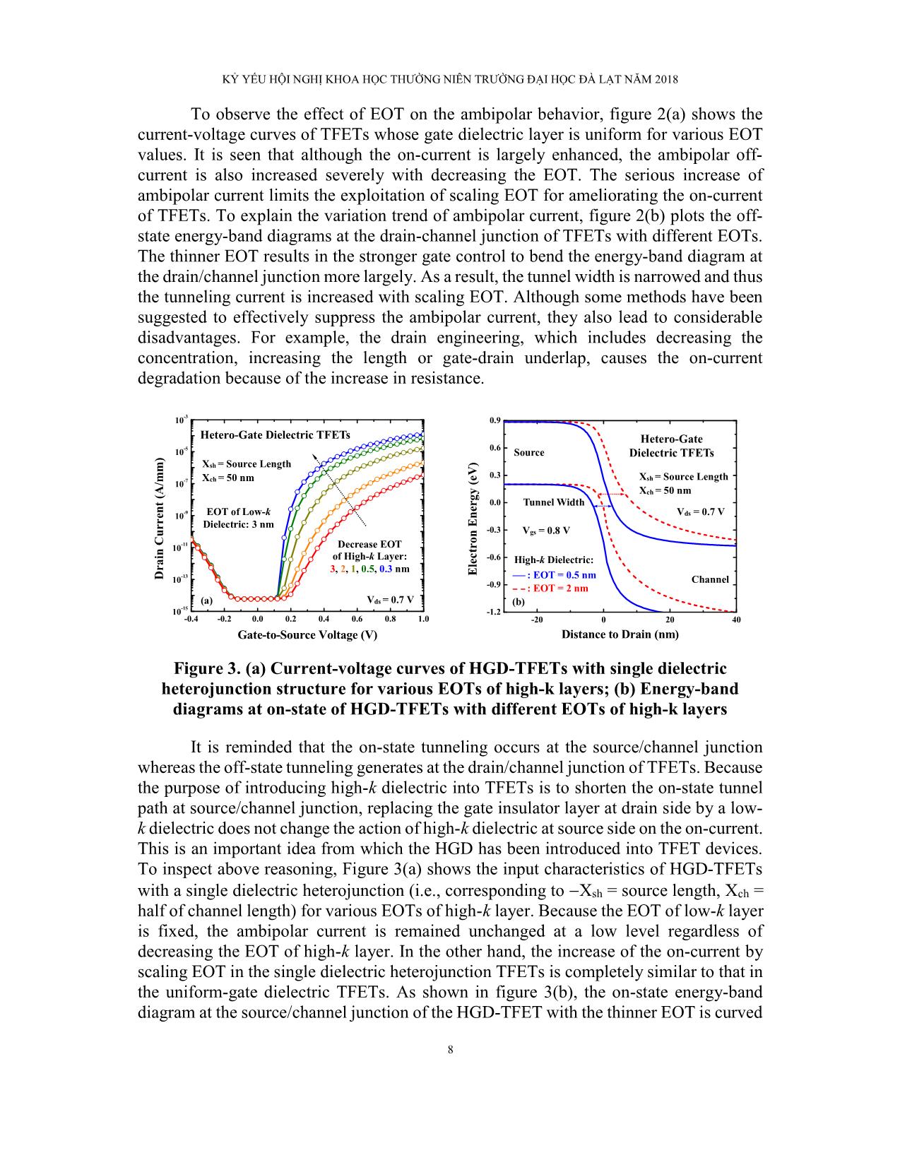
Trang 8
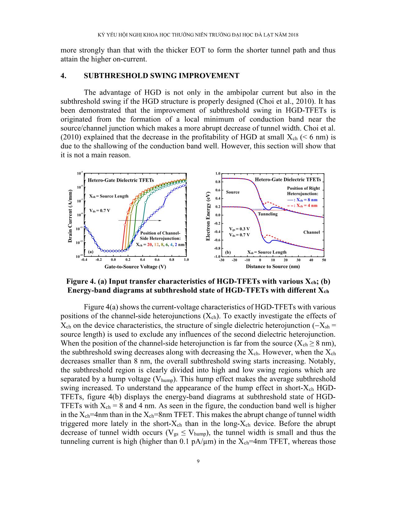
Trang 9
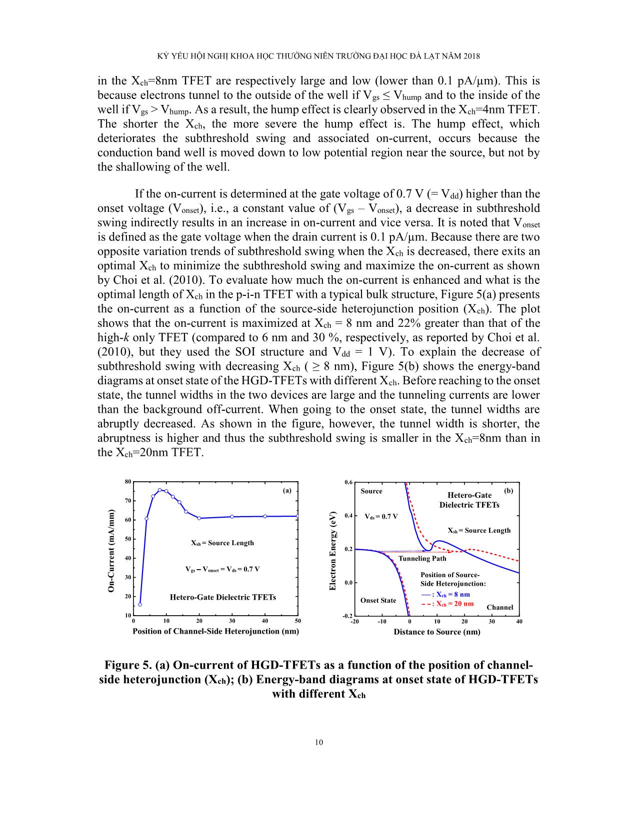
Trang 10
Tải về để xem bản đầy đủ
Tóm tắt nội dung tài liệu: Mechanisms of the performance enhancement by hetero - Gate dielectric in tunnel field - effect transistors
KỶ YẾU HỘI NGHỊ KHOA HỌC THƯỜNG NIÊN TRƯỜNG ĐẠI HỌC ĐÀ LẠT NĂM 2018
3
MECHANISMS OF THE PERFORMANCE ENHANCEMENT BY
HETERO-GATE DIELECTRIC IN TUNNEL FIELD-EFFECT
TRANSISTORS
Nguyen Dang Chiena , Ngo Thi Muaa, Tran Huu Duya, Chun-Hsing Shihb
aFaculty of Physics, Dalat University, Lam Dong, Vietnam
bDepartment of Electrical Engineering, National Chi Nan University, Nantou 54561, Taiwan
*Corresponding author: Email: chiennd@dlu.edu.vn
Abstract
The hetero-gate dielectric (HGD) structure has recently been demonstrated experimentally
in tunnel field-effect transistors (TFETs) to enhance their electrical performance. In this
paper, we adequately examine the mechanisms that the HGD works to ameliorate the
electrical characteristics of TFETs. A typical bulk p-i-n TFET structure is used to exclude
the uncertain effects of body factors on the role of HGD. It is showed that the subthreshold
swing is improved by the presence of a conduction band well near the source/channel
junction, but the swing improvement is limited by the appearance of the hump effect when
the local potential well approaches the source. By analyzing the roles of dielectric
heterojunctions at source- and channel-sides separately, it is found that the on-current
enhanced by the source-side heterojunction is about 5 times larger than by the channel-side
one. The reason is that the source-side heterojunction directly modulates the on-state tunnel
width, whereas the channel-side heterojunction indirectly affects the on-current through
modulating the subthreshold-state tunnel width. Exactly understanding the mechanisms of
the performance enhancement by HGD is important in studying the optimal design of HGD-
TFETs.
Keywords: Hetero-gate dielectric; high-k gate insulator; band-to-band tunneling; tunnel
field-effect transistor (TFET).
KỶ YẾU HỘI NGHỊ KHOA HỌC THƯỜNG NIÊN TRƯỜNG ĐẠI HỌC ĐÀ LẠT NĂM 2018
4
CƠ CHẾ NÂNG CAO ĐẶC TÍNH HOẠT ĐỘNG
NHỜ ĐIỆN MÔI CỰC CỔNG DỊ CHẤT TRONG TRANSISTOR
TRƯỜNG XUYÊN HẦM
Nguyễn Đăng Chiếna*, Ngô Thị Mùaa, Trần Hữu Duya, Chun-Hsing Shihb
a Khoa Vật lý, Trường Đại học Đà Lạt, Lâm Đồng, Việt Nam
bKhoa Kỹ Thuật Điện, Đại học Quốc lập Ký Nam, Nam Đầu, Đài Loan
*Tác giả liên hệ: Email: chiennd@dlu.edu.vn
Tóm tắt
Cấu trúc điện môi cực cổng dị chất (HGD) gần đây đã được chứng minh bằng thực nghiệm
trong các transistor trường xuyên hầm (TFET) để nâng cao đặc tính điện của chúng. Trong
bài báo này, chúng tôi nghiên cứu chi tiết các cơ chế giúp cho điện môi cực cổng dị chất có
thể cải thiện đặc tính điện của TFET. Cấu trúc p-i-n TFET khối đặc trưng được sử dụng để
loại trừ những ảnh hưởng không xác định của các yếu tố thân linh kiện đến vai trò của HGD.
Nghiên cứu chỉ ra rằng độ dốc dưới ngưỡng được cải thiện nhờ sự có mặt của một hố thế
định xứ gần chuyển tiếp nguồn/kênh, nhưng sự cải thiện này bị giới hạn bởi sự xuất hiện của
hiệu ứng bướu khi hố thế này tiến gần tới cực nguồn. Bằng việc phân tích vai trò của các
chuyển tiếp dị chất phía nguồn và kênh một cách riêng rẽ, nghiên cứu chỉ ra rằng dòng mở
được tăng lên nhờ chuyển tiếp dị chất phía nguồn lớn hơn khoảng 5 lần nhờ chuyển tiếp dị
chất phía kênh. Nguyên nhân là do chuyển tiếp dị chất phía nguồn hiệu chỉnh trực tiếp độ
rộng xuyên hầm ở trạng thái mở, trong khi chuyển tiếp dị chất phía kênh chỉ ảnh hưởng gián
tiếp tới dòng mở thông qua hiệu chỉnh độ rộng xuyên hầm ở trạng thái dưới ngưỡng. Việc
hiểu chính xác các cơ chế làm nâng cao đặc tính hoạt động của TFET nhờ cấu trúc HGD là
rất quan trọng trong quá trình thiết kế tối ưu cho các TFET có điện môi cực cổng dị chất.
Từ khóa: Điện môi cực cổng dị chất; chất cách điện có độ điện thẩm cao; xuyên hầm qua
vùng cấm; transistor trường xuyên hầm (TFET).
KỶ YẾU HỘI NGHỊ KHOA HỌC THƯỜNG NIÊN TRƯỜNG ĐẠI HỌC ĐÀ LẠT NĂM 2018
5
1. INTRODUCTION
Traditional metal-oxide-semiconductor field-effect transistors (MOSFETs) have
exhibited the unsuitability for use in ultra-low power applications since they are subjected
to the physical limit of 60 mV/decade subthreshold swing at room temperature
(International Technology Roadmap for Semiconductors, 2015). To overcome this
fundamental limit of MOSFETs, one has proposed tunnel field-effect transistors (TFETs)
whose steep on-off switching with sub-60 mV/decade subthreshold swing has been
experimentally demonstrated (Appenzeller et al., 2004; Choi et al., 2007). Other
significant advantages of TFETs over MOSFETs are small power dissipation (Koswatta
et al., 2009) and high dimensional scalability (Bardon et al., 2010). However, the band-
to-band tunneling, which makes the breakthrough of the kT/q limit, is also responsible for
low on-current in TFETs because the tunneling probability is relatively small (Seabaugh
& Zhang, 2010). Therefore, enhancing on-current has become the most challenge of
TFET devices and attracted much attention since the last 2000s.
In order to enhance the conduction current of TFETs, many methods relating to
both material and structure techniques have been proposed to reduce the tunnel barrier
and/or to increase the tunneling area at on-state (Nayfeh et al., 2009; Kao et al., 2012;
Chien et al., 2013). Since the tunneling probability is exponentially increased with
decreasing the height of tunnel barrier, using low-bandgap materials has been realized as
one of most effective techniques to boost the on-current (Nayfeh et al., 2009). In the other
hand, because of the same dependences of the tunneling probability on the width and the
height of tunnel barrier, narrowing the tunnel barrier has always be concerned largely.
While the tunnel barrier height is basically determined by the material bandgap, there are
so many factors that affect the tunnel barrier width such as source/drain doping profile
(Chien & Shih, 2017), gate insulator and spacer (Choi et al., 2016), gate materials (Noor
et al., 2017), body thickn ... G ĐẠI HỌC ĐÀ LẠT NĂM 2018
10
in the Xch=8nm TFET are respectively large and low (lower than 0.1 pA/µm). This is
because electrons tunnel to the outside of the well if Vgs ≤ Vhump and to the inside of the
well if Vgs > Vhump. As a result, the hump effect is clearly observed in the Xch=4nm TFET.
The shorter the Xch, the more severe the hump effect is. The hump effect, which
deteriorates the subthreshold swing and associated on-current, occurs because the
conduction band well is moved down to low potential region near the source, but not by
the shallowing of the well.
If the on-current is determined at the gate voltage of 0.7 V (= Vdd) higher than the
onset voltage (Vonset), i.e., a constant value of (Vgs – Vonset), a decrease in subthreshold
swing indirectly results in an increase in on-current and vice versa. It is noted that Vonset
is defined as the gate voltage when the drain current is 0.1 pA/µm. Because there are two
opposite variation trends of subthreshold swing when the Xch is decreased, there exits an
optimal Xch to minimize the subthreshold swing and maximize the on-current as shown
by Choi et al. (2010). To evaluate how much the on-current is enhanced and what is the
optimal length of Xch in the p-i-n TFET with a typical bulk structure, Figure 5(a) presents
the on-current as a function of the source-side heterojunction position (Xch). The plot
shows that the on-current is maximized at Xch = 8 nm and 22% greater than that of the
high-k only TFET (compared to 6 nm and 30 %, respectively, as reported by Choi et al.
(2010), but they used the SOI structure and Vdd = 1 V). To explain the decrease of
subthreshold swing with decreasing Xch ( ≥ 8 nm), Figure 5(b) shows the energy-band
diagrams at onset state of the HGD-TFETs with different Xch. Before reaching to the onset
state, the tunnel widths in the two devices are large and the tunneling currents are lower
than the background off-current. When going to the onset state, the tunnel widths are
abruptly decreased. As shown in the figure, however, the tunnel width is shorter, the
abruptness is higher and thus the subthreshold swing is smaller in the Xch=8nm than in
the Xch=20nm TFET.
0 10 20 30 40 50
10
20
30
40
50
60
70
80
O
n-
C
ur
re
nt
 (m
A
/m
m
)
Position of Channel-Side Heterojunction (nm)
Hetero-Gate Dielectric TFETs
Vgs Vonset = Vds = 0.7 V
(a)
Xsh = Source Length
-20 -10 0 10 20 30 40
-0.2
0.0
0.2
0.4
0.6
El
ec
tr
on
 E
ne
rg
y
(e
V
)
Distance to Source (nm)
Hetero-Gate
Dielectric TFETs
Onset State
Channel
(b) Source
Tunneling Path
: Xch = 8 nm
: Xch = 20 nm
Vds = 0.7 V
Position of Source-
Side Heterojunction:
Xsh = Source Length
Figure 5. (a) On-current of HGD-TFETs as a function of the position of channel-
side heterojunction (Xch); (b) Energy-band diagrams at onset state of HGD-TFETs
with different Xch
KỶ YẾU HỘI NGHỊ KHOA HỌC THƯỜNG NIÊN TRƯỜNG ĐẠI HỌC ĐÀ LẠT NĂM 2018
11
5. ON-CURRENT ENHANCEMENT
As shown in previous section, properly designing the position of channel-side
heterojunction (Xch) in HGD-TFETs can ameliorate the device on-current. However, the
on-current enhancement by optimizing Xch is relatively limited because (1) the on-current
is indirectly enhanced through the decrease of subthreshold swing and (2) the channel-
side heterojunction has to be kept far enough from the source/channel junction, where the
on-state tunneling occurs, to avoid the hump effect. It is inferred from this reasoning that
the on-current may be more significantly enhanced by optimally designing the source-
side dielectric heterojunction which is close to the source doping junction.
-0.4 -0.2 0.0 0.2 0.4 0.6 0.8 1.0
10-15
10-13
10-11
10-9
10-7
10-5
10-3
D
ra
in
 C
ur
re
nt
 (A
/m
m
)
Gate-to-Source Voltage (V)
Hetero-Gate Dielectric TFETs
Position of Source-
Side Heterojunction:
Circle : Xsh = 0 nm
Triangle : Xsh = 4 nm
Square : Xsh = 4 nm
Vds = 0.7 V
(a)
Xch = 50 nm
-10 -8 -6 -4 -2 0 2 4 6
0
20
40
60
80
100
120
140
O
n-
C
ur
re
nt
 (m
A
/m
m
)
Position of Source-Side Heterojunction (nm)
Hetero-Gate Dielectric TFETs
Vgs Vonset = Vds = 0.7 V
(b)
Xch = 50 nm
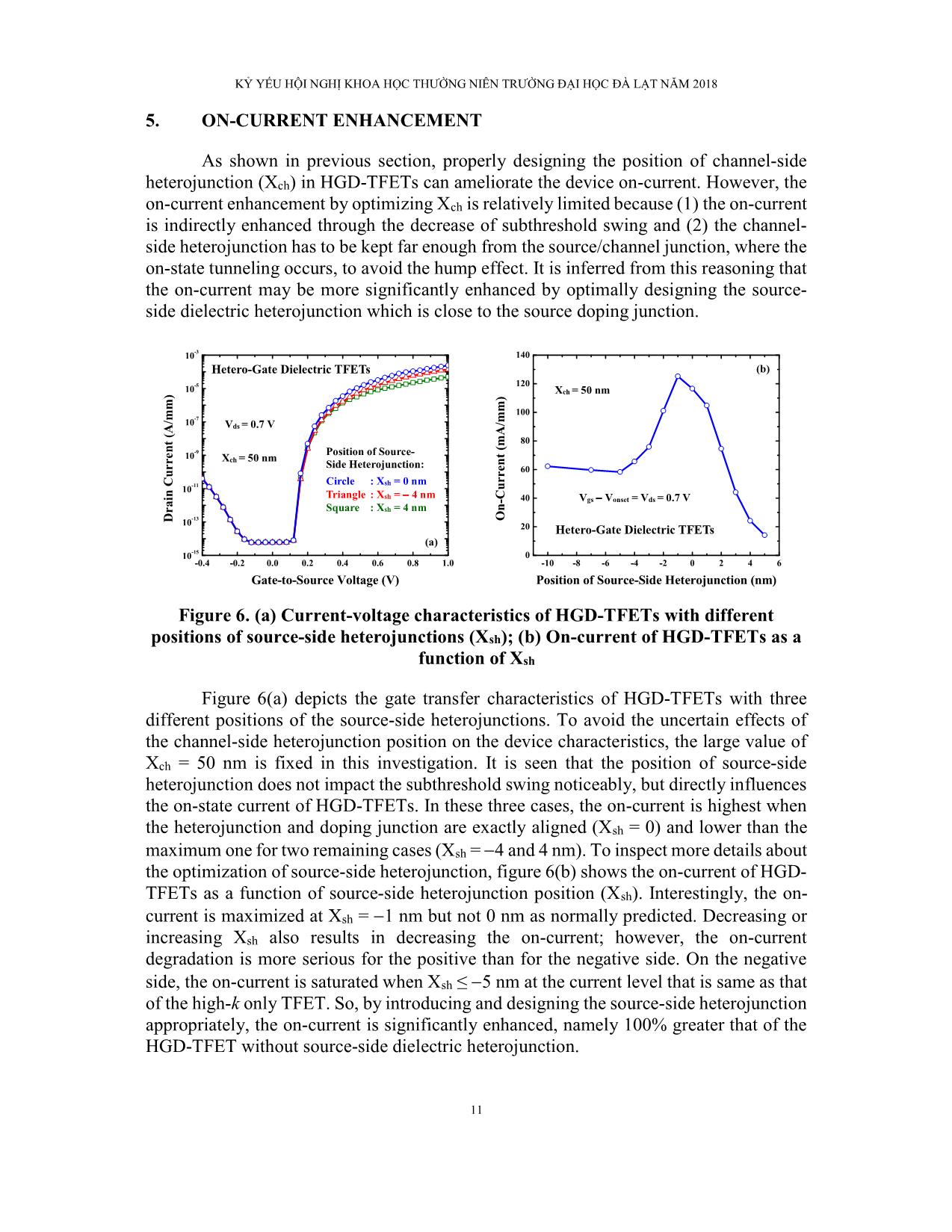
Figure 6. (a) Current-voltage characteristics of HGD-TFETs with different
positions of source-side heterojunctions (Xsh); (b) On-current of HGD-TFETs as a
function of Xsh
Figure 6(a) depicts the gate transfer characteristics of HGD-TFETs with three
different positions of the source-side heterojunctions. To avoid the uncertain effects of
the channel-side heterojunction position on the device characteristics, the large value of
Xch = 50 nm is fixed in this investigation. It is seen that the position of source-side
heterojunction does not impact the subthreshold swing noticeably, but directly influences
the on-state current of HGD-TFETs. In these three cases, the on-current is highest when
the heterojunction and doping junction are exactly aligned (Xsh = 0) and lower than the
maximum one for two remaining cases (Xsh = 4 and 4 nm). To inspect more details about
the optimization of source-side heterojunction, figure 6(b) shows the on-current of HGD-
TFETs as a function of source-side heterojunction position (Xsh). Interestingly, the on-
current is maximized at Xsh = 1 nm but not 0 nm as normally predicted. Decreasing or
increasing Xsh also results in decreasing the on-current; however, the on-current
degradation is more serious for the positive than for the negative side. On the negative
side, the on-current is saturated when Xsh ≤ 5 nm at the current level that is same as that
of the high-k only TFET. So, by introducing and designing the source-side heterojunction
appropriately, the on-current is significantly enhanced, namely 100% greater that of the
HGD-TFET without source-side dielectric heterojunction.
KỶ YẾU HỘI NGHỊ KHOA HỌC THƯỜNG NIÊN TRƯỜNG ĐẠI HỌC ĐÀ LẠT NĂM 2018
12
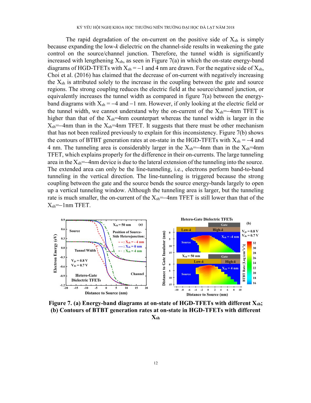
The rapid degradation of the on-current on the positive side of Xsh is simply
because expanding the low-k dielectric on the channel-side results in weakening the gate
control on the source/channel junction. Therefore, the tunnel width is significantly
increased with lengthening Xsh, as seen in Figure 7(a) in which the on-state energy-band
diagrams of HGD-TFETs with Xsh = 1 and 4 nm are drawn. For the negative side of Xsh,
Choi et al. (2016) has claimed that the decrease of on-current with negatively increasing
the Xsh is attributed solely to the increase in the coupling between the gate and source
regions. The strong coupling reduces the electric field at the source/channel junction, or
equivalently increases the tunnel width as compared in figure 7(a) between the energy-
band diagrams with Xsh = 4 and 1 nm. However, if only looking at the electric field or
the tunnel width, we cannot understand why the on-current of the Xsh= 4nm TFET is
higher than that of the Xsh=4nm counterpart whereas the tunnel width is larger in the
Xsh= 4nm than in the Xsh=4nm TFET. It suggests that there must be other mechanism
that has not been realized previously to explain for this inconsistency. Figure 7(b) shows
the contours of BTBT generation rates at on-state in the HGD-TFETs with Xsh = 4 and
4 nm. The tunneling area is considerably larger in the Xsh= 4nm than in the Xsh=4nm
TFET, which explains properly for the difference in their on-currents. The large tunneling
area in the Xsh= 4nm device is due to the lateral extension of the tunneling into the source.
The extended area can only be the line-tunneling, i.e., electrons perform band-to-band
tunneling in the vertical direction. The line-tunneling is triggered because the strong
coupling between the gate and the source bends the source energy-bands largely to open
up a vertical tunneling window. Although the tunneling area is larger, but the tunneling
rate is much smaller, the on-current of the Xsh= 4nm TFET is still lower than that of the
Xsh= 1nm TFET.
-20 -15 -10 -5 0 5 10 15 20
-1.2
-0.9
-0.6
-0.3
0.0
0.3
0.6
0.9
El
ec
tr
on
 E
ne
rg
y
(e
V
)
Distance to Source (nm)
Hetero-Gate
Dielectric TFETs
Vgs = 0.8 V
Vds = 0.7 V
Channel
(a)
Source
Tunnel Width
Position of Source-
Side Heterojunction:
: Xsh = - 4 nm
: Xsh = 0 nm
: Xsh = 4 nm
Xch = 50 nm
(b)
Distance to Source (nm)
0
5
-10
D
is
ta
nc
e
to
 G
at
e
In
su
la
to
r
(n
m
)
-8 -6 -4
Hetero-Gate Dielectric TFETs
Low-k
Source
10
15
-2 0
Vgs = 0.8 V
Vds = 0.7 V
High-k
Low-k High-k
Gate
Gate
0
5
10
15
2 4 6 8 10
Source 32
30
28
26
24
22
20
18
16
BT
BT
 R
at
e
[L
og
 (c
m
-3
s-1
)]
Xsh = -4 nm
Xsh = 4 nm
Xch = 50 nm
Figure 7. (a) Energy-band diagrams at on-state of HGD-TFETs with different Xsh;
(b) Contours of BTBT generation rates at on-state in HGD-TFETs with different
Xsh
KỶ YẾU HỘI NGHỊ KHOA HỌC THƯỜNG NIÊN TRƯỜNG ĐẠI HỌC ĐÀ LẠT NĂM 2018
13
6. CONCLUSION
By using two-dimensional numerical simulations, the device physics of HGD-
TFETs has been explored to achieve an adequate understanding on the mechanisms of
how the TFET performance is enhanced by the HGD. The suppression of detrimental
hump effect, which emerges in HGD-TFETs with a short high-k layer, is expected to
exploit the benefit of HGD effectively. In addition, the source-side heterojunction has to
be more carefully designed and fabricated because the on-current of HGD-TFETs is more
sensitive on the position of the source- than on the channel-side heterojunction.
ACKNOWLEDGMENTS
This research is funded by the Ministry of Education & Training and Dalat
University, Vietnam. This work is also supported by the National Center for High-
Performance Computing of Taiwan.
REFERENCES
Appenzeller, J., Lin, Y.-M., Knoch, J., & Avouris Ph. (2004). Band-to-band tunneling in
carbon nanotube field-effect transistors! Phys. Rev. Lett., 93(19), 196905.
Bardon, M. G., Neves, H. P., Puers R., & Hoof, C. V. (2010). Pseudo-two-dimensional
model for double-gate tunnel FETs considering the junctions depletion regions!
IEEE Trans. Electron Devices, 57(4), 827-834.
Boucart, K. & Ionescu, A. M. (2007). Double-gate tunnel FET with high-κ gate dielectric!
IEEE Trans. Electron Devices, 54(7), 1725-1733.
Chien, N.D. & Shih, C.-H. (2016). Short channel effects in tunnel field-effect transistors
with different configurations of abrupt and graded Si/SiGe heterojunctions,
Superlattices Microstruct., 100, 857-866.
Chien, N.D. & Shih, C.-H. (2017). Oxide thickness-dependent effects of source doping
profile on the performance of single- and double-gate tunnel field-effect
transistors! Superlattices Microstruct., 102, 284-299.
Chien, N.D., Shih, C.-H., & Vinh, L.T. (2013). Drive current enhancement in tunnel field-
effect transistors by graded heterojunction approach! J. Appl. Phys., 114(9),
094507 [Erratum! 114(18), 189901].
Chien, N.D., Shih, C.-H., Chen, Y.-H., & Thu, N.T. (2016, January). Increasing drain
voltage of low-bandgap tunnel field-effect transistors by drain engineering.
Presented at the International Conference Electronics, Information and
Communications, Vietnam. Retrieved from
Choi, W. Y. & Lee, H. K. (2016). Demonstration of hetero-gate-dielectric tunneling field-
effect transistors (HG TFETs)! Nano Convergence, 3(1), 1-15.
Choi, W. Y. & Lee, W. (2010). Hetero-gate-dielectric tunneling field-effect transistors!
KỶ YẾU HỘI NGHỊ KHOA HỌC THƯỜNG NIÊN TRƯỜNG ĐẠI HỌC ĐÀ LẠT NĂM 2018
14
IEEE Trans. Electron Devices, 57(9), 2317-2319.
Choi, W. Y., Park, B.-G., Lee, J. D., & Liu, T.-J. K. (2007). Tunneling field-effect
transistors (TFETs) with subthreshold swing (SS) less than 60 mV/dec! IEEE
Electron Device Lett., 28(8), 743-745.
International Technology Roadmap for Semiconductors. More Moore. (2015) (available
at
Kao, K.-H., Verhulst, A.S., Vandenberghe, W.G., Soree, B., Groeseneken, G., & Meyer,
K.D. (2012). Direct and indirect band-to-band tunneling in germanium-based
TFETs! IEEE Trans. Electron Devices, 59(2), 292-301.
Koswatta, S.O., Lundstrom, M.S., & Nikonov, D.E. (2009). Performance comparison
between p-i-n tunneling transistors and conventional MOSFETs! IEEE Trans.
Electron Devices, 56(3), 456-465.
Mohata, D., Mookerjea, S., Agrawal, A., Li, Y., Mayer, T., Narayanan, V., Liu, A.,
Loubychev, D., Fastenau, J., & Datta, S. (2011). Experimental staggered-source
and N+ pocket-doped channel III–V tunnel field-effect transistors and their
scalabilities! Appl. Phys. Exp., 4 (2) 024105.
Nayfeh, O. M., Hoyt, J. L., & Antoniadis, D. A. (2009). Strained-Si1-xGex/Si band-to-
band tunneling transistors: Impact of tunnel junction germanium composition and
doping concentration on switching behavior! IEEE Trans. Electron Devices,
56(10), 2264-2269.
Noor, S. L., Safa, S., & Khan, Md. Z. R. (2017). A silicon-based dual-material double-
gate TFET with optimized performance! Int. J. Numer. Model. Electronic
Networks, Devices and Fields, 30(6), e2220.
Seabaugh, A. C. & Zhang, Q. (2010). Low voltage tunnel transistors for beyond CMOS
logic! Proceedings of the IEEE, 98(12), 2095-2110.
Synopsys MEDICI User’s Manual (California: Synopsys Inc.). 2010.
Toh, E.-H., Wang, G. H., Chan, L., Samudra, G., & Yeo, Y.-C. (2007). Device physics
and design of double-gate tunneling field-effect transistor by silicon film
thickness optimization! Appl. Phys. Lett., 90(26), 263507.
Vandenberghe W. G., Verhulst A. S., Groeseneken G., Soree B., & Magnus W. (2008,
September). Analytical model for point and line tunneling in a tunnel field-effect
transistor. Paper presented at the International Conference on Simulation of
Semiconductor Processes and Devices, Japan. Retrieved from
File đính kèm:
 mechanisms_of_the_performance_enhancement_by_hetero_gate_die.pdf

