Design and analysis of 10 nm T-Gate enhancement-mode MOS-HEMT for high power microwave applications
In this work, we propose a novel enhancement-mode GaN metal-oxide-semiconductor high electron
mobility transistor (MOS-HEMT) with a 10 nm T-gate length and a high-k TiO2 gate dielectric. The DC and
RF characteristics of the proposed GaN MOS-HEMT structure are analyzed by using a TCAD Software. The
device features are heavily doped (nþþ GaN) source/drain regions for reducing the contact resistances
and gate capacitances, which uplift the microwave characteristics of the MOS-HEMT. The enhancementmode GaN MOS-HEMTs showed an outstanding performance with a threshold voltage of 1.07 V,
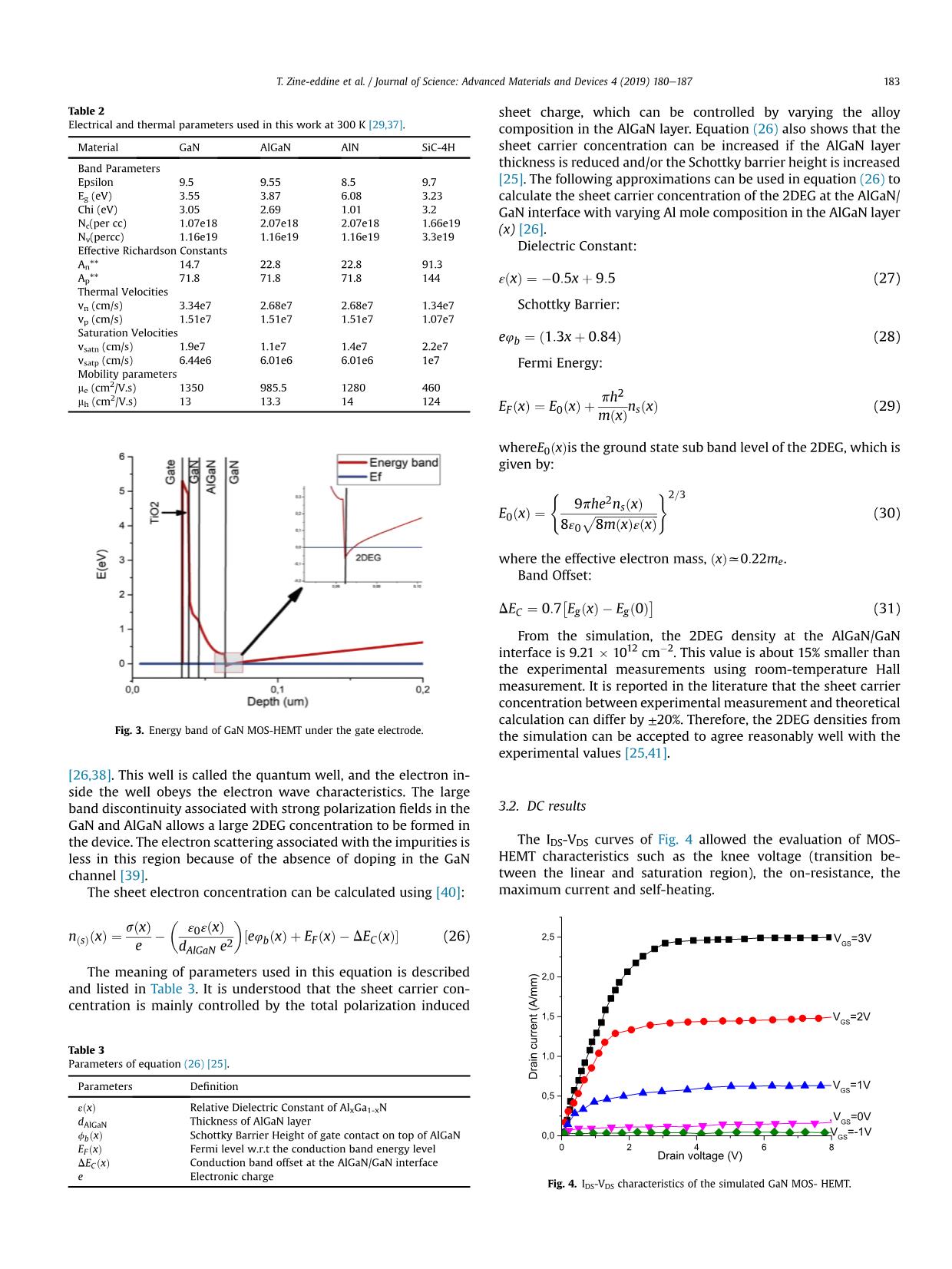
maximum extrinsic transconductance of 1438 mS/mm, saturation current at VGS ¼ 2 V of 1.5 A/mm,
maximum current of 2.55 A/mm, unity-gain cut-off frequency of 524 GHz, and with a record maximum
oscillation frequency of 758 GHz. The power performance characterized at 10 GHz to give an output
power of 29.6 dBm, a power gain of 24.2 dB, and a power-added efficiency of 43.1%. Undoubtedly, these
results place the device at the forefront for high power and millimeter wave applications
Trang 1
Trang 2
Trang 3
Trang 4
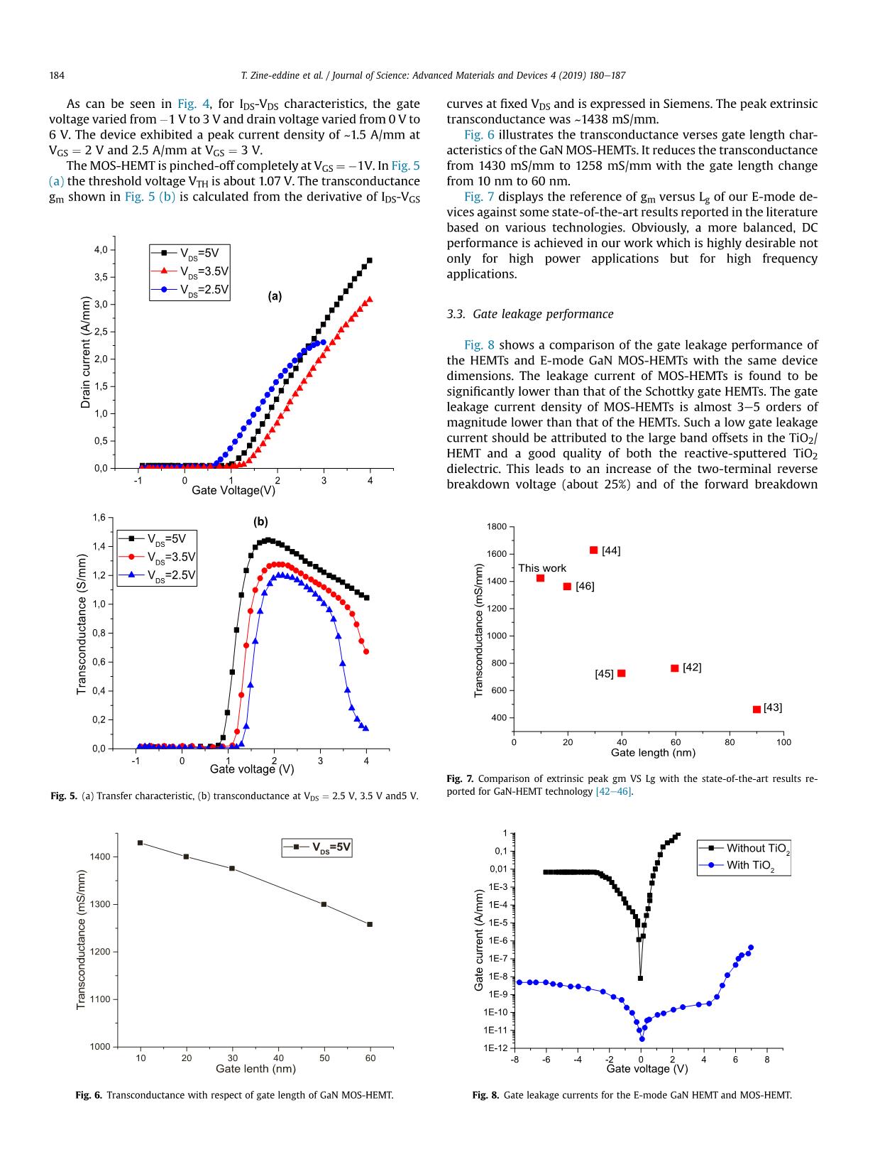
Trang 5
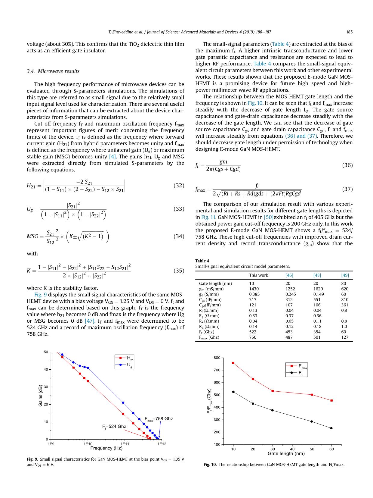
Trang 6
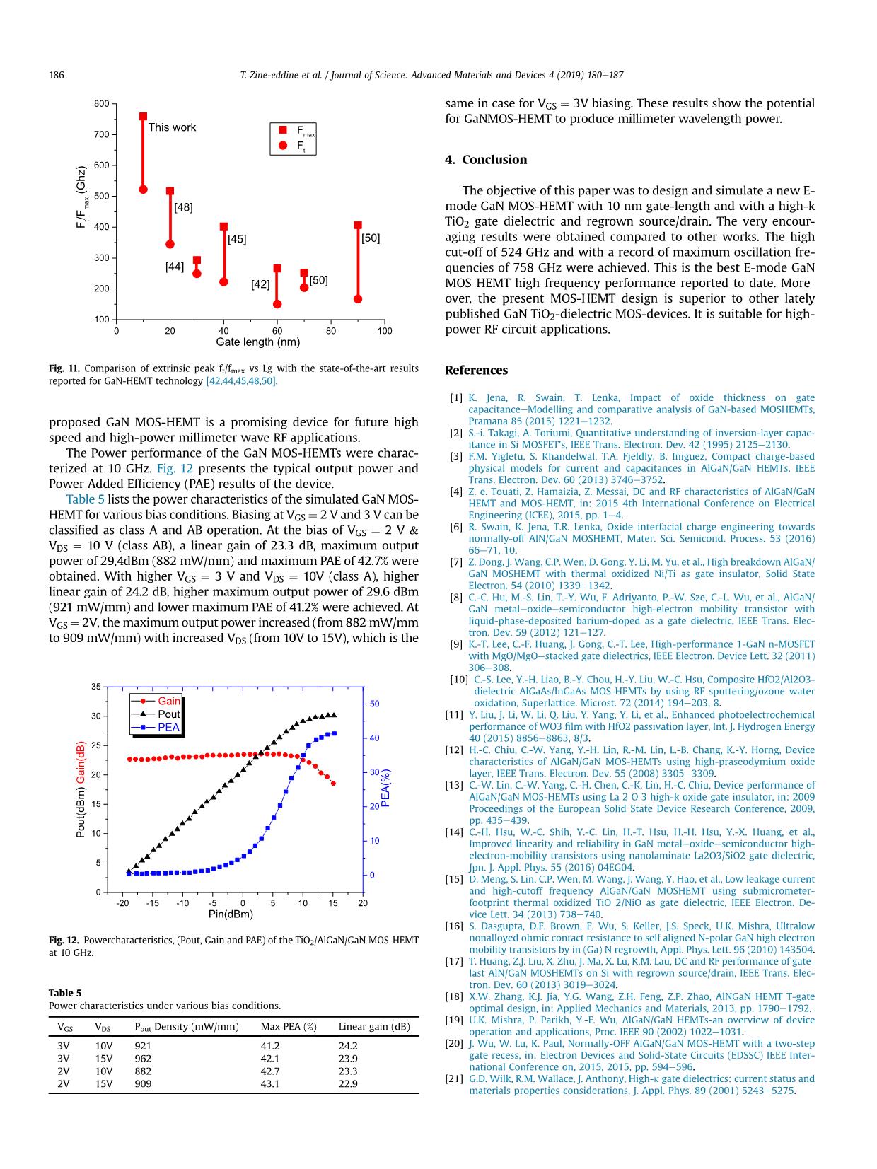
Trang 7
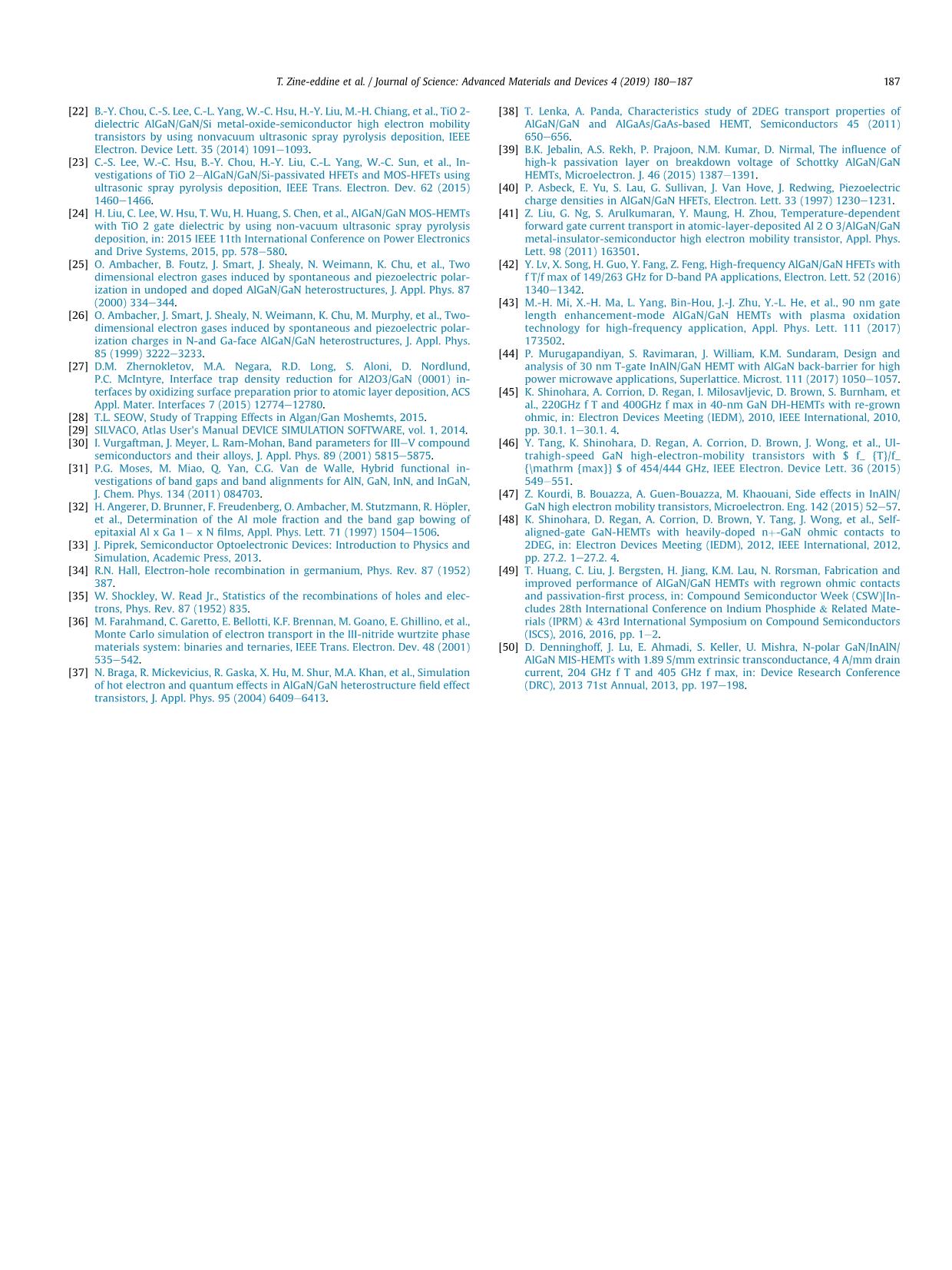
Trang 8
Tóm tắt nội dung tài liệu: Design and analysis of 10 nm T-Gate enhancement-mode MOS-HEMT for high power microwave applications
atou
Bisk
Received in revised form
a n
EM
RF characteristics of the proposed GaN MOS-HEMT structure are analyzed by using a TCAD Software. The
and gate capacitances, which uplift the microwave characteristics of the MOS-HEMT. The enhancement-
y trans
[10,11], Pr2O3 [12,13], SiN [14], SiO2 [14] and NiO [15] as the gate
ntact resistance of
U mm due to the
ce-drain distance.
in ohmic contacts
resistivity in the
duces the gate ac-
le maintaining the
e capacitance [18].
d HEMTs [19] and
zations for two-dimensional electron gas (2DEG) formation [19].
Although these types of devices were used in microwave power
amplifiers, low noise and RF switching devices, enhancement-
mode MOS-HEMTs [17,20] have added a more advantage in
simpler circuit design and low power consumption due to the
elimination of negative power supply [17] which is suitable for the
radio frequency integrated circuit (RFIC) design. In this paper, we
* Corresponding author. Laboratory of Semiconducting and Metallic Materials,
University of Mohamed Khider Biskra, Algeria
E-mail addresses: zinouu113@yahoo.fr (T. Zine-eddine), hamaiziaz@gmail.com
(H. Zahra), messaimr@yahoo.fr (M. Zitouni).
Contents lists available at ScienceDirect
Journal of Science: Advanc
journal homepage: www.el
Journal of Science: Advanced Materials and Devices 4 (2019) 180e187Peer review under responsibility of Vietnam National University, Hanoi.insulating dielectric is widely investigated, and excellent perfor-
mance is demonstrated utilizing Al2O3 [4,6], TiO2 [7e9], HfO2
MOS-HEMTs [17] are the depletion type due to their unique ma-
terial properties leading to spontaneous and piezoelectric polari-down voltage, high saturation velocity, low effective mass, high
thermal conductivity and high two-dimensional electron gas (2DEG)
density of the order of 1013 cm2 at the hetero interface [1e3].
However, Schottky gate transistors usually exhibit a high gate
leakage current [4], and a drain current collapse when operating at
high frequencies. These are the major factors that limit the perfor-
mance and reliability of HEMT in radio frequency (RF) power
applications.
Metal oxide semiconductor HEMTs (MOS-HEMTs) with an
All these devices suffered from the high co
>0.3 U mm and the high on-resistance of >1
alloyed ohmic contacts and the large sour
Recently, the heavily doped n þ GaN source/dra
allowed a significant reduction of the contact
proposed device [16,17]. The T-gate structure re
cess resistance by providing a large gate areawhi
smaller gate length and reduces the extrinsic gat
Also, most of the developed AlGaN/GaN basemost preferred devices for high-power and high frequency applica-
tions, due to their suitable material properties such as high break-
voltage (Vth). The dielectric with high permittivity (high k) can
effectively alleviate these problems.Keywords:
Enhancement-mode
MOS-HEMT
High-k
TiO2
Regrown source/drain
TCAD
1. Introduction
GaN-based high electron mobilithttps://doi.org/10.1016/j.jsamd.2019.01.001
2468-2179/© 2019 The Authors. Publishing services b
( extrinsic transconductance of 1438 mS/mm, saturation current at VGS ¼ 2 V of 1.5 A/mm,
maximum current of 2.55 A/mm, unity-gain cut-off frequency of 524 GHz, and with a record maximum
oscillation frequency of 758 GHz. The power performance characterized at 10 GHz to give an output
power of 29.6 dBm, a power gain of 24.2 dB, and a power-added efficiency of 43.1%. Undoubtedly, these
results place the device at the forefront for high power and millimeter wave applications.
© 2019 The Authors. Publishing services by Elsevier B.V. on behalf of Vietnam National University, Hanoi.
This is an open access article under the CC BY license (
istors (HEMTs) are the
dielectric to overcome the aforementioned limitation. These solu-
tions, however, were performed at the expense of a decrease in the
device transconductance (gm) and large shift in the thresholdAccepted 2 January 2019
Available online 7 January 2019mode GaN MOS-HEMTs showed an outstanding performance with a threshold voltage of 1.07 V,30 December 2018 device features are heavily doped (nþþ GaN) source/drain regions for reducing the contact resistancesOriginal Article
Design and analysis of 10 nm T-gate enh
for high power microwave applications
Touati Zine-eddine a, *, Hamaizia Zahra a, Messai Zi
a Laboratory of Semiconducting and Metallic Materials, University of Mohamed Khider
b Electronics Department, Faculty of Sciences and Technology, University of BBA, Algeria
c Laboratory of Optoelectronics and Components, UFAS 19000, Algeria
a r t i c l e i n f o
Article history:
Received 17 December 2018
a b s t r a c t
In this work, we propose
mobility transistor (MOS-Hy Elsevier B.V. on behalf of Vietnamncement-mode MOS-HEMT
ni b, c
ra, Algeria
ovel enhancement-mode GaN metal-oxide-semiconductor high electron
T) with a 10 nm T-gate length and a high-k TiO2 gate dielectric. The DC and
ed Materials and Devices
sevier .com/locate/ jsamdNational University, Hanoi. This is an open access article under the CC BY license
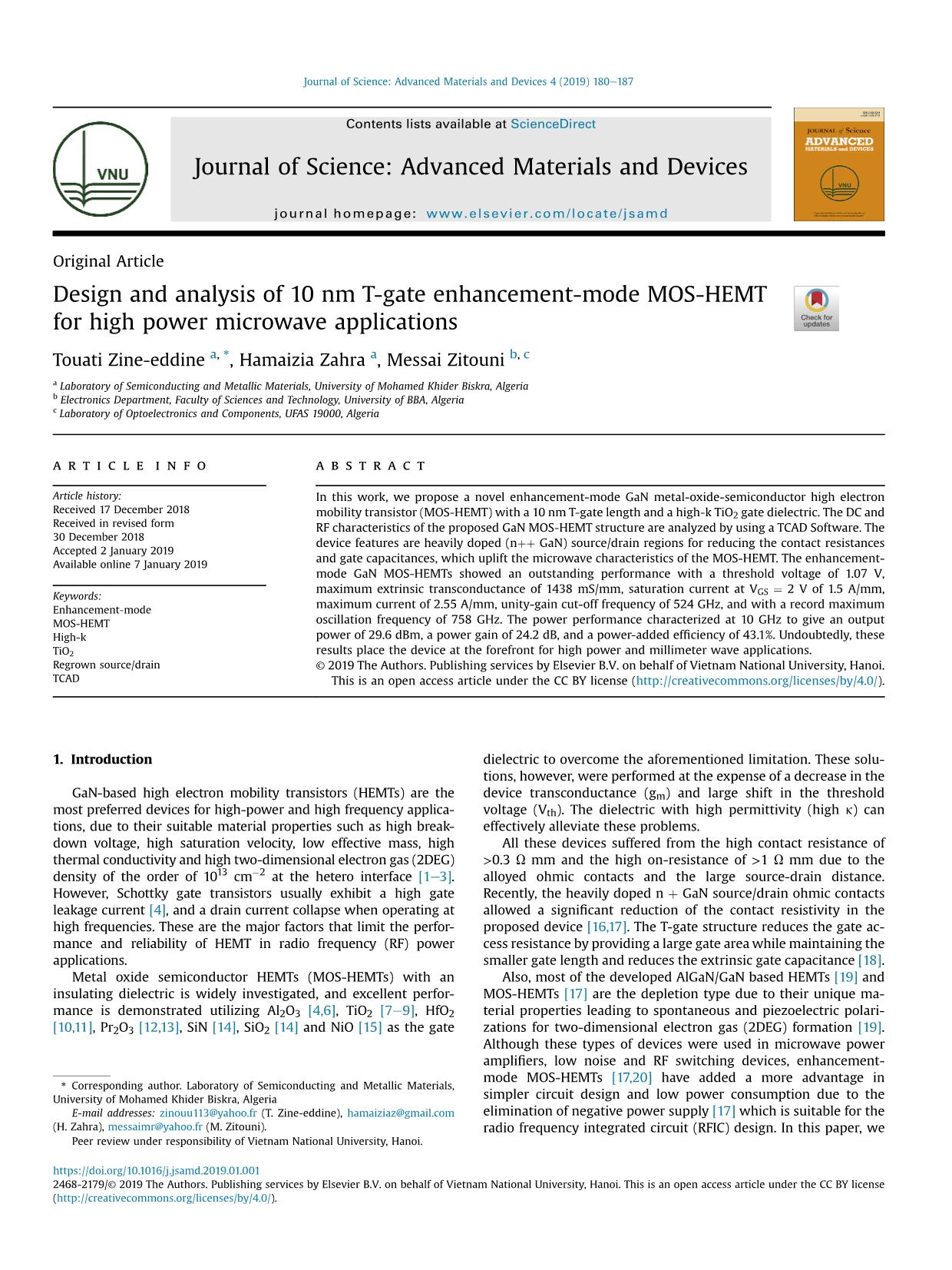
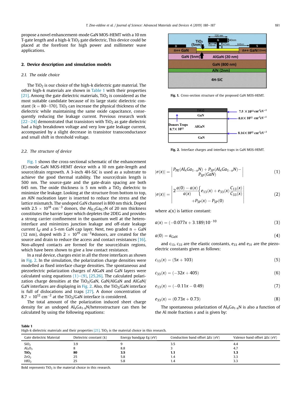
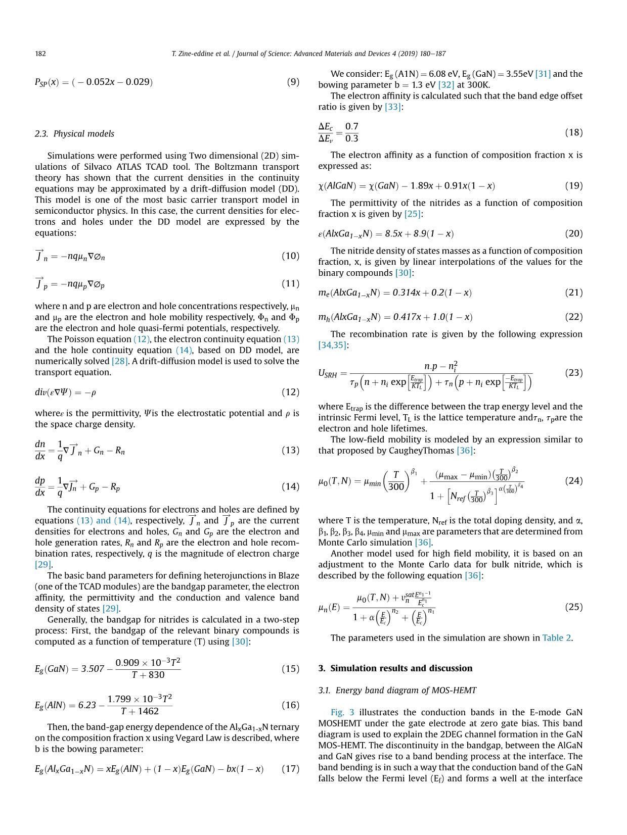
propose a novel enhancement-mode GaNMOS-HEMTwith a 10 nm
T-gate length and a high-k TiO2 gate dielectric, This device could be
placed at the forefront for high power and millimeter wave
applications.
2. Device description and simulation models
2.1. The oxide choice
which have been shown to give a low contact resistance.
að0Þ ¼ aGaN (4)
and c13, c33 are the elastic constants, e33 and e31 are the piezo-
electric constants given as follows:
c13ðxÞ ¼ ð5xþ 103Þ (5)
c33ðxÞ ¼ ð32xþ 405Þ (6)
e13ðxÞ ¼ ð0:11x 0:49Þ (7)
e33ðxÞ ¼ ð0:73xþ 0:73Þ (8)
The spontaneous polarization of AlxGa1-xN is also a function of
the Al mole fraction x and is given by:
his research.
Gate dielectric Material Dielectric constant (k) Energy bandgap Eg (eV) Conduction band offset DEc (eV) Valence band offset DEc (eV)
3.5 4.4
3 4.7
1.1 1.3
1.4 3.3
1.4 3.3
T. Zine- ... S22j2 þ jS11S22  S12S21j2
2 jS12j2  jS22j2
(35)
where K is the stability factor.
Fig. 9 displays the small signal characteristics of the same MOS-
HEMT device with a bias voltage VGS ¼ 1.25 V and VDS ¼ 6 V. ft and
fmax can be determined based on this graph; fT is the frequency
value where h21 becomes 0 dB and fmax is the frequency where Ug
or MSG becomes 0 dB [47]. fT and fmax were determined to be
524 GHz and a record of maximum oscillation frequency (fmax) of
758 GHz.
10
20
30
40
50
Fmax=758 Ghz
G
ai
ns
 (d
B
)
 H21
 Ug
Ft=524 GhzFig. 9. Small signal characteristics for GaN MOS-HEMT at the bias point VGS ¼ 1.35 V
and VDS ¼ 6 V.Table 4
Small-signal equivalent circuit model parameters.
This work [46] [48] [49]
Gate length (nm) 10 20 20 80
gm (mS/mm) 1430 1252 1620 620
gd (S/mm) 0.385 0.245 0.149 60
Cgs (fF/mm) 317 312 551 810
Cgd(fF/mm) 121 107 106 361
Ri (U.mm) 0.13 0.04 0.04 0.8
Rg (U.mm) 0.33 0.37 0.36 e
Rs (U.mm) 0.04 0.05 0.11 0.8
Rd (U.mm) 0.14 0.12 0.18 1.0
Ft (Ghz) 522 453 354 60
Fmax (Ghz) 750 487 501 127
10 20 30 40 50 60
100
200
300
400
500
600
700
800
Gate length (nm)
F t
/F
m
ax
 (G
hz
)
 Fmax
 FtFig. 10. The relationship between GaN MOS-HEMT gate length and Ft/Fmax.
proposed GaN MOS-HEMT is a promising device for future high
speed and high-power millimeter wave RF applications.
The Power performance of the GaN MOS-HEMTs were charac-
terized at 10 GHz. Fig. 12 presents the typical output power and
Power Added Efficiency (PAE) results of the device.
Table 5 lists the power characteristics of the simulated GaNMOS-
HEMT for various bias conditions. Biasing at V ¼ 2 V and 3 V can be
0 20 40 60 80 100
100
200
300
400
500
600
700
800
[50][45]
[42] [50]
[44]
F t
/F
m
ax
 (G
hz
)
Gate length (nm)
 Fmax
 Ft
[48]
This work
Fig. 11. Comparison of extrinsic peak ft/fmax vs Lg with the state-of-the-art results
reported for GaN-HEMT technology [42,44,45,48,50].
T. Zine-eddine et al. / Journal of Science: Advanc186GS
classified as class A and AB operation. At the bias of VGS ¼ 2 V &
VDS ¼ 10 V (class AB), a linear gain of 23.3 dB, maximum output
power of 29,4dBm (882 mW/mm) and maximum PAE of 42.7% were
obtained. With higher VGS ¼ 3 V and VDS ¼ 10V (class A), higher
linear gain of 24.2 dB, higher maximum output power of 29.6 dBm
(921 mW/mm) and lower maximum PAE of 41.2% were achieved. At
VGS¼ 2V, themaximumoutput power increased (from 882mW/mm
to 909 mW/mm) with increased VDS (from 10V to 15V), which is the
25
30
35
Gain
 Pout
PEA
dB
) 40
50pp. 435e439.
[19] U.K. Mishra, P. Parikh, Y.-F. Wu, AlGaN/GaN HEMTs-an overview of device
operation and applications, Proc. IEEE 90 (2002) 1022e1031.
-20 -15 -10 -5 0 5 10 15 20
0
5
10
15
20
Pin(dBm)
P
ou
t(d
B
m
) G
ai
n(
0
10
20
30
 P
E
A
(%
)
Fig. 12. Powercharacteristics, (Pout, Gain and PAE) of the TiO2/AlGaN/GaN MOS-HEMT
at 10 GHz.
Table 5
Power characteristics under various bias conditions.
VGS VDS Pout Density (mW/mm) Max PEA (%) Linear gain (dB)
3V 10V 921 41.2 24.2
3V 15V 962 42.1 23.9
2V 10V 882 42.7 23.3
2V 15V 909 43.1 22.9[20] J. Wu, W. Lu, K. Paul, Normally-OFF AlGaN/GaN MOS-HEMT with a two-step
gate recess, in: Electron Devices and Solid-State Circuits (EDSSC) IEEE Inter-
national Conference on, 2015, 2015, pp. 594e596.[14] C.-H. Hsu, W.-C. Shih, Y.-C. Lin, H.-T. Hsu, H.-H. Hsu, Y.-X. Huang, et al.,
Improved linearity and reliability in GaN metaleoxideesemiconductor high-
electron-mobility transistors using nanolaminate La2O3/SiO2 gate dielectric,
Jpn. J. Appl. Phys. 55 (2016) 04EG04.
[15] D. Meng, S. Lin, C.P. Wen, M. Wang, J. Wang, Y. Hao, et al., Low leakage current
and high-cutoff frequency AlGaN/GaN MOSHEMT using submicrometer-
footprint thermal oxidized TiO 2/NiO as gate dielectric, IEEE Electron. De-
vice Lett. 34 (2013) 738e740.
[16] S. Dasgupta, D.F. Brown, F. Wu, S. Keller, J.S. Speck, U.K. Mishra, Ultralow
nonalloyed ohmic contact resistance to self aligned N-polar GaN high electron
mobility transistors by in (Ga) N regrowth, Appl. Phys. Lett. 96 (2010) 143504.
[17] T. Huang, Z.J. Liu, X. Zhu, J. Ma, X. Lu, K.M. Lau, DC and RF performance of gate-
last AlN/GaN MOSHEMTs on Si with regrown source/drain, IEEE Trans. Elec-
tron. Dev. 60 (2013) 3019e3024.
[18] X.W. Zhang, K.J. Jia, Y.G. Wang, Z.H. Feng, Z.P. Zhao, AlNGaN HEMT T-gate
optimal design, in: Applied Mechanics and Materials, 2013, pp. 1790e1792.same in case for VGS ¼ 3V biasing. These results show the potential
for GaNMOS-HEMT to produce millimeter wavelength power.
4. Conclusion
The objective of this paper was to design and simulate a new E-
mode GaN MOS-HEMT with 10 nm gate-length and with a high-k
TiO2 gate dielectric and regrown source/drain. The very encour-
aging results were obtained compared to other works. The high
cut-off of 524 GHz and with a record of maximum oscillation fre-
quencies of 758 GHz were achieved. This is the best E-mode GaN
MOS-HEMT high-frequency performance reported to date. More-
over, the present MOS-HEMT design is superior to other lately
published GaN TiO2-dielectric MOS-devices. It is suitable for high-
power RF circuit applications.
References
[1] K. Jena, R. Swain, T. Lenka, Impact of oxide thickness on gate
capacitanceeModelling and comparative analysis of GaN-based MOSHEMTs,
Pramana 85 (2015) 1221e1232.
[2] S.-i. Takagi, A. Toriumi, Quantitative understanding of inversion-layer capac-
itance in Si MOSFET's, IEEE Trans. Electron. Dev. 42 (1995) 2125e2130.
[3] F.M. Yigletu, S. Khandelwal, T.A. Fjeldly, B. I~niguez, Compact charge-based
physical models for current and capacitances in AlGaN/GaN HEMTs, IEEE
Trans. Electron. Dev. 60 (2013) 3746e3752.
[4] Z. e. Touati, Z. Hamaizia, Z. Messai, DC and RF characteristics of AlGaN/GaN
HEMT and MOS-HEMT, in: 2015 4th International Conference on Electrical
Engineering (ICEE), 2015, pp. 1e4.
[6] R. Swain, K. Jena, T.R. Lenka, Oxide interfacial charge engineering towards
normally-off AlN/GaN MOSHEMT, Mater. Sci. Semicond. Process. 53 (2016)
66e71, 10.
[7] Z. Dong, J. Wang, C.P. Wen, D. Gong, Y. Li, M. Yu, et al., High breakdown AlGaN/
GaN MOSHEMT with thermal oxidized Ni/Ti as gate insulator, Solid State
Electron. 54 (2010) 1339e1342.
[8] C.-C. Hu, M.-S. Lin, T.-Y. Wu, F. Adriyanto, P.-W. Sze, C.-L. Wu, et al., AlGaN/
GaN metaleoxideesemiconductor high-electron mobility transistor with
liquid-phase-deposited barium-doped as a gate dielectric, IEEE Trans. Elec-
tron. Dev. 59 (2012) 121e127.
[9] K.-T. Lee, C.-F. Huang, J. Gong, C.-T. Lee, High-performance 1-GaN n-MOSFET
with MgO/MgOestacked gate dielectrics, IEEE Electron. Device Lett. 32 (2011)
306e308.
[10] C.-S. Lee, Y.-H. Liao, B.-Y. Chou, H.-Y. Liu, W.-C. Hsu, Composite HfO2/Al2O3-
dielectric AlGaAs/InGaAs MOS-HEMTs by using RF sputtering/ozone water
oxidation, Superlattice. Microst. 72 (2014) 194e203, 8.
[11] Y. Liu, J. Li, W. Li, Q. Liu, Y. Yang, Y. Li, et al., Enhanced photoelectrochemical
performance of WO3 film with HfO2 passivation layer, Int. J. Hydrogen Energy
40 (2015) 8856e8863, 8/3.
[12] H.-C. Chiu, C.-W. Yang, Y.-H. Lin, R.-M. Lin, L.-B. Chang, K.-Y. Horng, Device
characteristics of AlGaN/GaN MOS-HEMTs using high-praseodymium oxide
layer, IEEE Trans. Electron. Dev. 55 (2008) 3305e3309.
[13] C.-W. Lin, C.-W. Yang, C.-H. Chen, C.-K. Lin, H.-C. Chiu, Device performance of
AlGaN/GaN MOS-HEMTs using La 2 O 3 high-k oxide gate insulator, in: 2009
Proceedings of the European Solid State Device Research Conference, 2009,
ed Materials and Devices 4 (2019) 180e187[21] G.D. Wilk, R.M. Wallace, J. Anthony, High-k gate dielectrics: current status and
materials properties considerations, J. Appl. Phys. 89 (2001) 5243e5275.
[22] B.-Y. Chou, C.-S. Lee, C.-L. Yang, W.-C. Hsu, H.-Y. Liu, M.-H. Chiang, et al., TiO 2-
dielectric AlGaN/GaN/Si metal-oxide-semiconductor high electron mobility
transistors by using nonvacuum ultrasonic spray pyrolysis deposition, IEEE
Electron. Device Lett. 35 (2014) 1091e1093.
[23] C.-S. Lee, W.-C. Hsu, B.-Y. Chou, H.-Y. Liu, C.-L. Yang, W.-C. Sun, et al., In-
vestigations of TiO 2eAlGaN/GaN/Si-passivated HFETs and MOS-HFETs using
ultrasonic spray pyrolysis deposition, IEEE Trans. Electron. Dev. 62 (2015)
1460e1466.
[24] H. Liu, C. Lee, W. Hsu, T. Wu, H. Huang, S. Chen, et al., AlGaN/GaN MOS-HEMTs
with TiO 2 gate dielectric by using non-vacuum ultrasonic spray pyrolysis
deposition, in: 2015 IEEE 11th International Conference on Power Electronics
and Drive Systems, 2015, pp. 578e580.
[25] O. Ambacher, B. Foutz, J. Smart, J. Shealy, N. Weimann, K. Chu, et al., Two
dimensional electron gases induced by spontaneous and piezoelectric polar-
ization in undoped and doped AlGaN/GaN heterostructures, J. Appl. Phys. 87
(2000) 334e344.
[26] O. Ambacher, J. Smart, J. Shealy, N. Weimann, K. Chu, M. Murphy, et al., Two-
dimensional electron gases induced by spontaneous and piezoelectric polar-
ization charges in N-and Ga-face AlGaN/GaN heterostructures, J. Appl. Phys.
85 (1999) 3222e3233.
[27] D.M. Zhernokletov, M.A. Negara, R.D. Long, S. Aloni, D. Nordlund,
P.C. McIntyre, Interface trap density reduction for Al2O3/GaN (0001) in-
terfaces by oxidizing surface preparation prior to atomic layer deposition, ACS
Appl. Mater. Interfaces 7 (2015) 12774e12780.
[28] T.L. SEOW, Study of Trapping Effects in Algan/Gan Moshemts, 2015.
[29] SILVACO, Atlas User's Manual DEVICE SIMULATION SOFTWARE, vol. 1, 2014.
[30] I. Vurgaftman, J. Meyer, L. Ram-Mohan, Band parameters for IIIeV compound
semiconductors and their alloys, J. Appl. Phys. 89 (2001) 5815e5875.
[31] P.G. Moses, M. Miao, Q. Yan, C.G. Van de Walle, Hybrid functional in-
vestigations of band gaps and band alignments for AlN, GaN, InN, and InGaN,
J. Chem. Phys. 134 (2011) 084703.
[32] H. Angerer, D. Brunner, F. Freudenberg, O. Ambacher, M. Stutzmann, R. H€opler,
et al., Determination of the Al mole fraction and the band gap bowing of
epitaxial Al x Ga 1 x N films, Appl. Phys. Lett. 71 (1997) 1504e1506.
[33] J. Piprek, Semiconductor Optoelectronic Devices: Introduction to Physics and
Simulation, Academic Press, 2013.
[38] T. Lenka, A. Panda, Characteristics study of 2DEG transport properties of
AlGaN/GaN and AlGaAs/GaAs-based HEMT, Semiconductors 45 (2011)
650e656.
[39] B.K. Jebalin, A.S. Rekh, P. Prajoon, N.M. Kumar, D. Nirmal, The influence of
high-k passivation layer on breakdown voltage of Schottky AlGaN/GaN
HEMTs, Microelectron. J. 46 (2015) 1387e1391.
[40] P. Asbeck, E. Yu, S. Lau, G. Sullivan, J. Van Hove, J. Redwing, Piezoelectric
charge densities in AlGaN/GaN HFETs, Electron. Lett. 33 (1997) 1230e1231.
[41] Z. Liu, G. Ng, S. Arulkumaran, Y. Maung, H. Zhou, Temperature-dependent
forward gate current transport in atomic-layer-deposited Al 2 O 3/AlGaN/GaN
metal-insulator-semiconductor high electron mobility transistor, Appl. Phys.
Lett. 98 (2011) 163501.
[42] Y. Lv, X. Song, H. Guo, Y. Fang, Z. Feng, High-frequency AlGaN/GaN HFETs with
f T/f max of 149/263 GHz for D-band PA applications, Electron. Lett. 52 (2016)
1340e1342.
[43] M.-H. Mi, X.-H. Ma, L. Yang, Bin-Hou, J.-J. Zhu, Y.-L. He, et al., 90 nm gate
length enhancement-mode AlGaN/GaN HEMTs with plasma oxidation
technology for high-frequency application, Appl. Phys. Lett. 111 (2017)
173502.
[44] P. Murugapandiyan, S. Ravimaran, J. William, K.M. Sundaram, Design and
analysis of 30 nm T-gate InAlN/GaN HEMT with AlGaN back-barrier for high
power microwave applications, Superlattice. Microst. 111 (2017) 1050e1057.
[45] K. Shinohara, A. Corrion, D. Regan, I. Milosavljevic, D. Brown, S. Burnham, et
al., 220GHz f T and 400GHz f max in 40-nm GaN DH-HEMTs with re-grown
ohmic, in: Electron Devices Meeting (IEDM), 2010, IEEE International, 2010,
pp. 30.1. 1e30.1. 4.
[46] Y. Tang, K. Shinohara, D. Regan, A. Corrion, D. Brown, J. Wong, et al., Ul-
trahigh-speed GaN high-electron-mobility transistors with $ f_ {T}/f_
{\mathrm {max}} $ of 454/444 GHz, IEEE Electron. Device Lett. 36 (2015)
549e551.
[47] Z. Kourdi, B. Bouazza, A. Guen-Bouazza, M. Khaouani, Side effects in InAlN/
GaN high electron mobility transistors, Microelectron. Eng. 142 (2015) 52e57.
[48] K. Shinohara, D. Regan, A. Corrion, D. Brown, Y. Tang, J. Wong, et al., Self-
aligned-gate GaN-HEMTs with heavily-doped nþ-GaN ohmic contacts to
2DEG, in: Electron Devices Meeting (IEDM), 2012, IEEE International, 2012,
pp. 27.2. 1e27.2. 4.
[49] T. Huang, C. Liu, J. Bergsten, H. Jiang, K.M. Lau, N. Rorsman, Fabrication and
T. Zine-eddine et al. / Journal of Science: Advanced Materials and Devices 4 (2019) 180e187 187[34] R.N. Hall, Electron-hole recombination in germanium, Phys. Rev. 87 (1952)
387.
[35] W. Shockley, W. Read Jr., Statistics of the recombinations of holes and elec-
trons, Phys. Rev. 87 (1952) 835.
[36] M. Farahmand, C. Garetto, E. Bellotti, K.F. Brennan, M. Goano, E. Ghillino, et al.,
Monte Carlo simulation of electron transport in the III-nitride wurtzite phase
materials system: binaries and ternaries, IEEE Trans. Electron. Dev. 48 (2001)
535e542.
[37] N. Braga, R. Mickevicius, R. Gaska, X. Hu, M. Shur, M.A. Khan, et al., Simulation
of hot electron and quantum effects in AlGaN/GaN heterostructure field effect
transistors, J. Appl. Phys. 95 (2004) 6409e6413.improved performance of AlGaN/GaN HEMTs with regrown ohmic contacts
and passivation-first process, in: Compound Semiconductor Week (CSW)[In-
cludes 28th International Conference on Indium Phosphide & Related Mate-
rials (IPRM) & 43rd International Symposium on Compound Semiconductors
(ISCS), 2016, 2016, pp. 1e2.
[50] D. Denninghoff, J. Lu, E. Ahmadi, S. Keller, U. Mishra, N-polar GaN/InAlN/
AlGaN MIS-HEMTs with 1.89 S/mm extrinsic transconductance, 4 A/mm drain
current, 204 GHz f T and 405 GHz f max, in: Device Research Conference
(DRC), 2013 71st Annual, 2013, pp. 197e198.
File đính kèm:
 design_and_analysis_of_10_nm_t_gate_enhancement_mode_mos_hem.pdf

