Effect of annealing temperature on the structure of ZnO films
In this work, ZnO nanocrystalline thin films were obtained by evaporating Zn
using the thermal evaporation technique and then thermal treatment. The results show that
after annealed at temperature of 400°C, the porous structure becomes visible and the ZnO
film has a particle-like structure. At an annealing temperature of 450°C, the film has a
flower-like structure. The smoother and approximately uniform surface can be observed at
an annealing temperature of 500°C. The film goes into state of compression with decrease
in annealing temperature from 500ºC to 350ºC and becomes completely stress free at about
485ºC. The lattice constant c increases from 5.1992 Å to 5.2020 Å on increasing the
thickness from 600 nm to 1200 nm and the stress gradually decreases. This implies that the
stress film can be relaxed by increasing the film thickness. The obtained ZnO films were
characterized by X-ray diffraction (XRD) and a field emission scanning electron
microscope (FE-SEM).
Trang 1
Trang 2
Trang 3
Trang 4
Trang 5
Trang 6
Trang 7
Trang 8

Trang 9
Tóm tắt nội dung tài liệu: Effect of annealing temperature on the structure of ZnO films
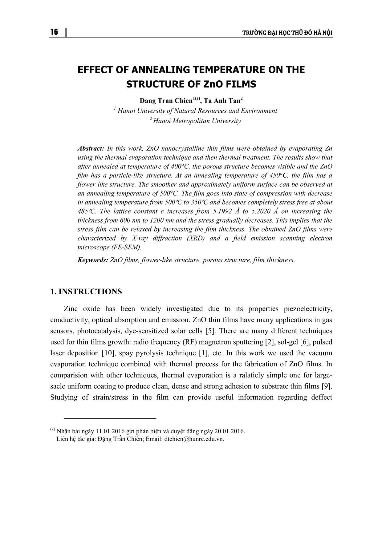
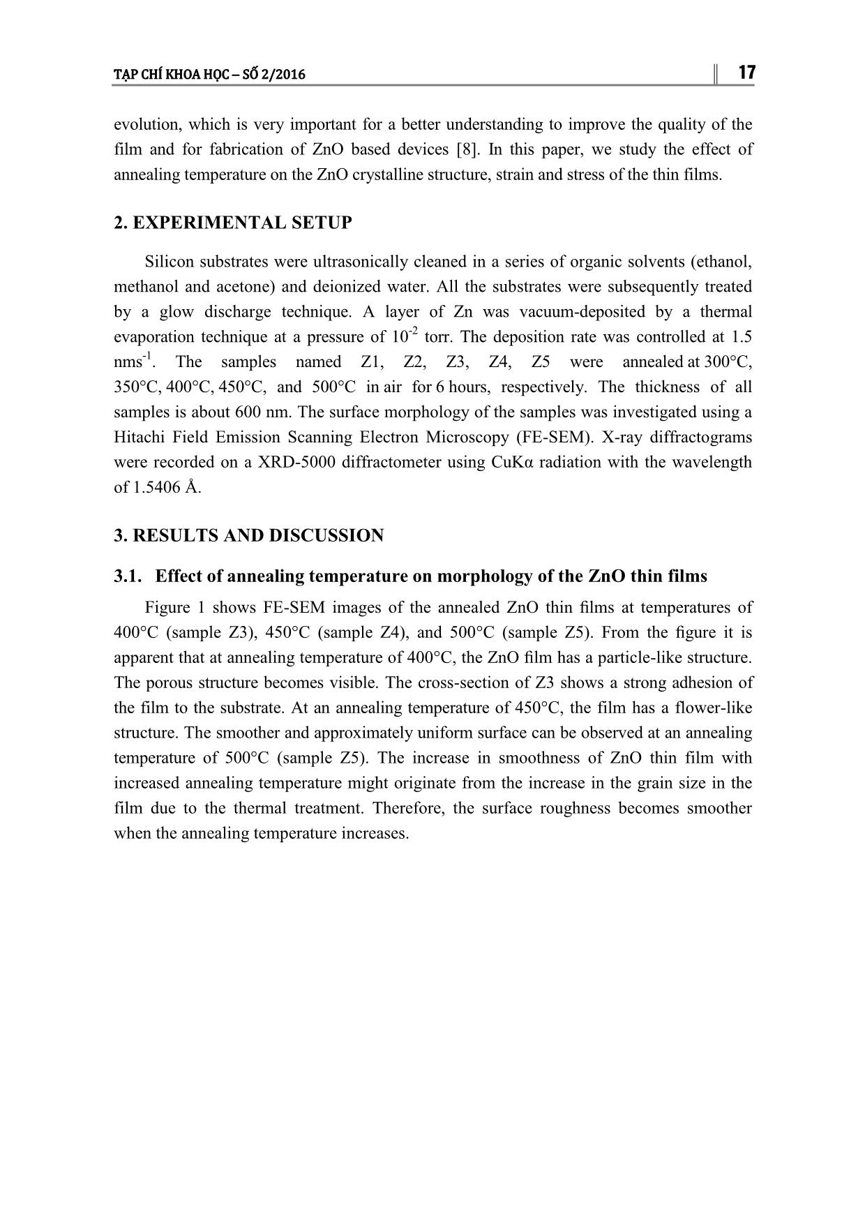
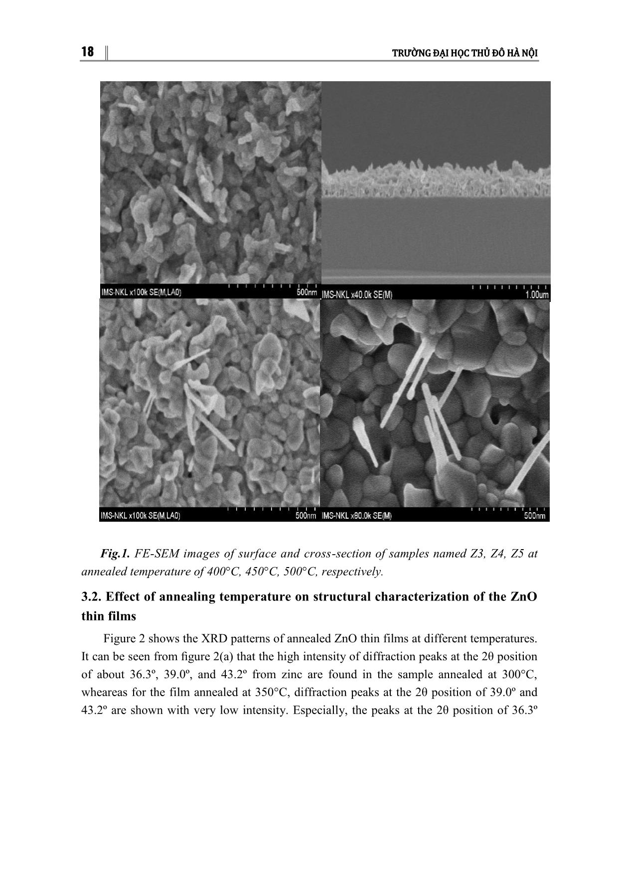
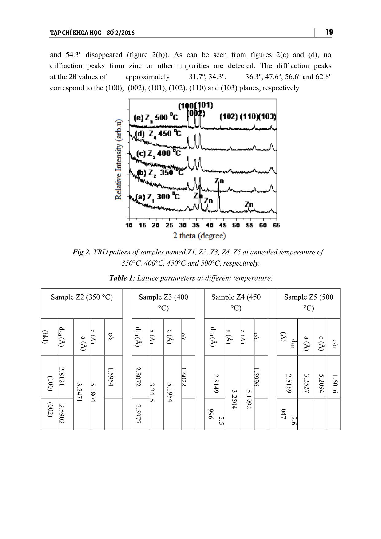
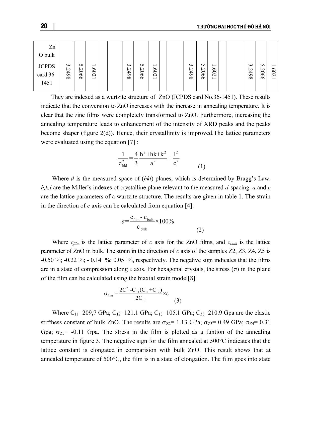
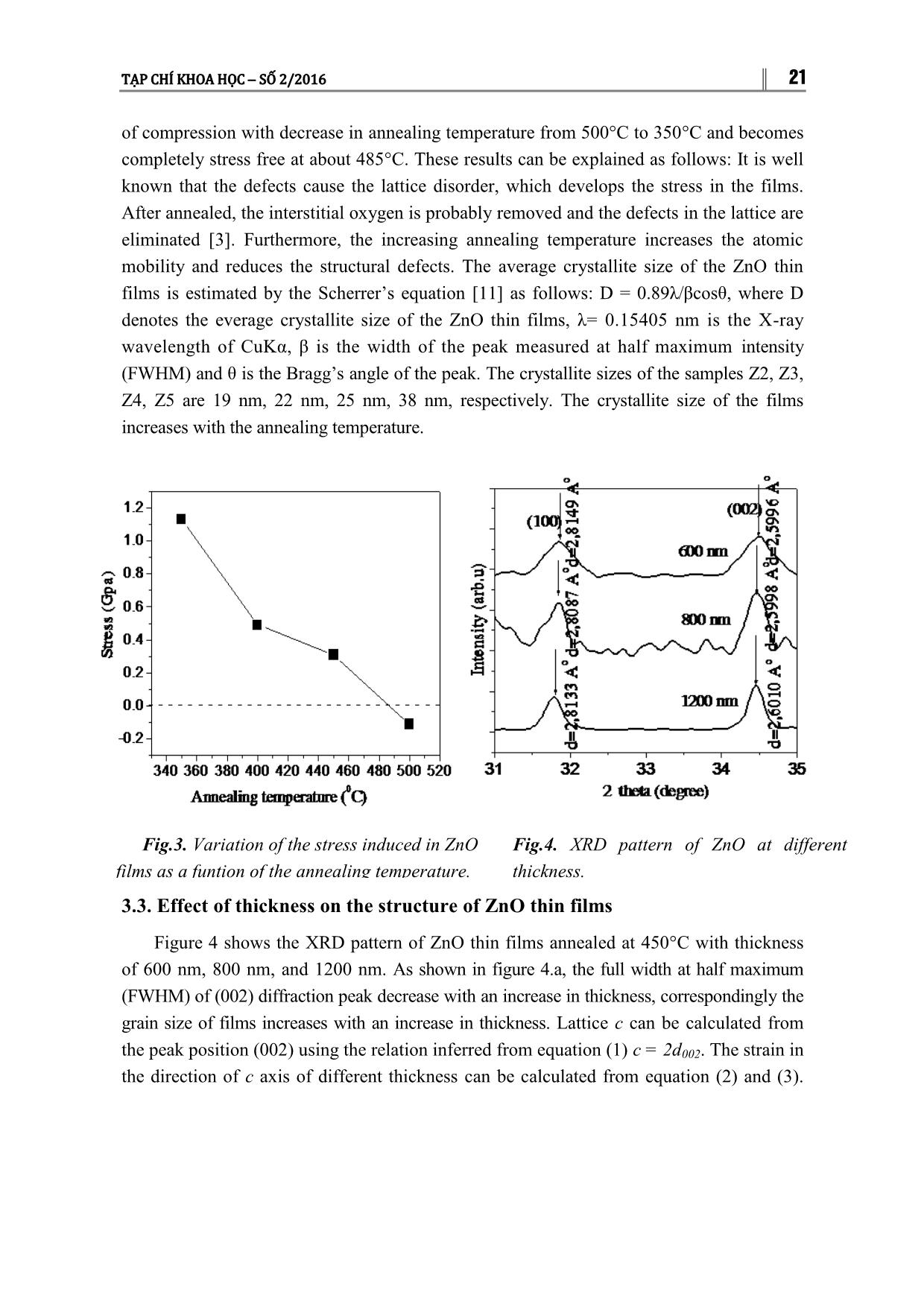
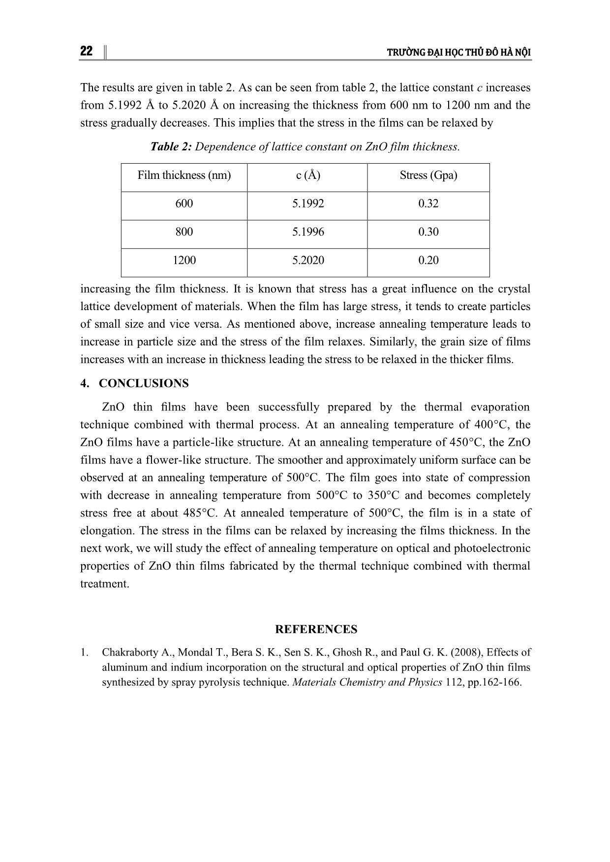
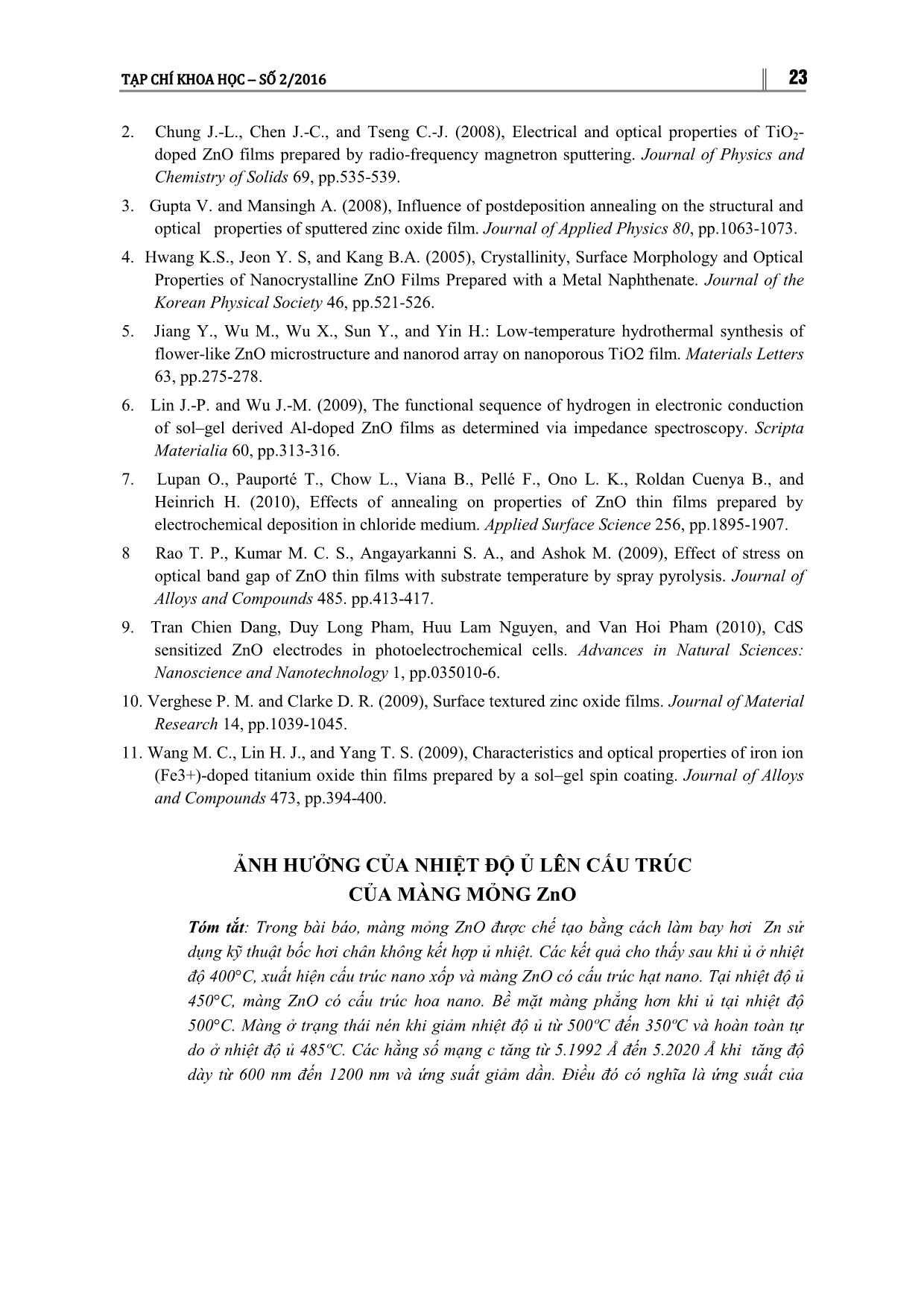
16 TRƯỜNG ĐẠI HỌC THỦ ĐÔ HÀ NỘI EFFECT OF ANNEALING TEMPERATURE ON THE STRUCTURE OF ZnO FILMS Dang Tran Chien 1(1) , Ta Anh Tan 2 1 Hanoi University of Natural Resources and Environment 2 Hanoi Metropolitan University Abstract: In this work, ZnO nanocrystalline thin films were obtained by evaporating Zn using the thermal evaporation technique and then thermal treatment. The results show that after annealed at temperature of 400°C, the porous structure becomes visible and the ZnO film has a particle-like structure. At an annealing temperature of 450°C, the film has a flower-like structure. The smoother and approximately uniform surface can be observed at an annealing temperature of 500°C. The film goes into state of compression with decrease in annealing temperature from 500ºC to 350ºC and becomes completely stress free at about 485ºC. The lattice constant c increases from 5.1992 Å to 5.2020 Å on increasing the thickness from 600 nm to 1200 nm and the stress gradually decreases. This implies that the stress film can be relaxed by increasing the film thickness. The obtained ZnO films were characterized by X-ray diffraction (XRD) and a field emission scanning electron microscope (FE-SEM). Keywords: ZnO films, flower-like structure, porous structure, film thickness. 1. INSTRUCTIONS Zinc oxide has been widely investigated due to its properties piezoelectricity, conductivity, optical absorption and emission. ZnO thin films have many applications in gas sensors, photocatalysis, dye-sensitized solar cells [5]. There are many different techniques used for thin films growth: radio frequency (RF) magnetron sputtering [2], sol-gel [6], pulsed laser deposition [10], spay pyrolysis technique [1], etc. In this work we used the vacuum evaporation technique combined with thermal process for the fabrication of ZnO films. In comparision with other techniques, thermal evaporation is a ralatiely simple one for large- sacle uniform coating to produce clean, dense and strong adhesion to substrate thin films [9]. Studying of strain/stress in the film can provide useful information regarding deffect (1) Nhận bài ngày 11.01.2016 gửi phản biện và duyệt đăng ngày 20.01.2016. Liên hệ tác giả: Đặng Trần Chiến; Email: dtchien@hunre.edu.vn. TẠP CHÍ KHOA HỌC SỐ 2/2016 17 evolution, which is very important for a better understanding to improve the quality of the film and for fabrication of ZnO based devices [8]. In this paper, we study the effect of annealing temperature on the ZnO crystalline structure, strain and stress of the thin films. 2. EXPERIMENTAL SETUP Silicon substrates were ultrasonically cleaned in a series of organic solvents (ethanol, methanol and acetone) and deionized water. All the substrates were subsequently treated by a glow discharge technique. A layer of Zn was vacuum-deposited by a thermal evaporation technique at a pressure of 10 -2 torr. The deposition rate was controlled at 1.5 nms -1 . The samples named Z1, Z2, Z3, Z4, Z5 were annealed at 300°C, 350°C, 400°C, 450°C, and 500°C in air for 6 hours, respectively. The thickness of all samples is about 600 nm. The surface morphology of the samples was investigated using a Hitachi Field Emission Scanning Electron Microscopy (FE-SEM). X-ray diffractograms were recorded on a XRD-5000 diffractometer using CuKα radiation with the wavelength of 1.5406 Å. 3. RESULTS AND DISCUSSION 3.1. Effect of annealing temperature on morphology of the ZnO thin films Figure 1 shows FE-SEM images of the annealed ZnO thin films at temperatures of 400°C (sample Z3), 450°C (sample Z4), and 500°C (sample Z5). From the figure it is apparent that at annealing temperature of 400°C, the ZnO film has a particle-like structure. The porous structure becomes visible. The cross-section of Z3 shows a strong adhesion of the film to the substrate. At an annealing temperature of 450°C, the film has a flower-like structure. The smoother and approximately uniform surface can be observed at an annealing temperature of 500°C (sample Z5). The increase in smoothness of ZnO thin film with increased annealing temperature might originate from the increase in the grain size in the film due to the thermal treatment. Therefore, the surface roughness becomes smoother when the annealing temperature increases. 18 TRƯỜNG ĐẠI HỌC THỦ ĐÔ HÀ NỘI Fig.1. FE-SEM images of surface and cross-section of samples named Z3, Z4, Z5 at annealed temperature of 400°C, 450°C, 500°C, respectively. 3.2. Effect of annealing temperature on structural characterization of the ZnO thin films Figure 2 shows the XRD patterns of annealed ZnO thin films at different temperatures. It can be seen from figure 2(a) that the high intensity of diffraction peaks at the 2θ position of about 36.3º, 39.0º, and 43.2º from zinc are found in the sample annealed at 300°C, wheareas for the film annealed at 350°C, diffraction peaks at the 2θ position of 39.0º and 43.2º are shown with very low intensity. Especially, the peaks at the 2θ position of 36.3º TẠP CHÍ KHOA HỌC SỐ 2/2016 19 and 54.3º disappeared (figure 2(b)). As can be seen from figures 2(c) and (d), no diffraction peaks from zinc or other impurities are detected. The diffraction peaks at the 2θ values of approximately 31.7º, 34.3º, 36.3º, 47.6º, 56.6º and 62.8º correspond to the (100), (002), (101), (102), (110) and (103) planes, respectively. Fig.2. XRD pattern of samples named Z1, Z2, Z3, Z4, Z5 at annealed temperature of 350°C, 400°C, 450°C and 500°C, respectively. Table 1: Lattice parameters at different temperature. Sample Z2 (350 °C) Sample Z3 (400 °C) Sample Z4 (450 °C) Sample Z5 (500 °C) (h k l) d h k l (Å ) a (Å ) c (Å ) c/a d h k l (Å ) a (Å ) c (Å ) c/a d h k l (Å ) a (Å ) c (Å ) c/a d h k l (Å ) a (Å ) c (Å ) c/a (1 0 0 ) 2 .8 1 2 1 3 .2 4 7 1 5 .1 8 0 4 1 .5 9 5 4 2 .8 0 7 2 3 .2 4 1 5 5 .1 9 5 4 1 .6 0 2 8 2 .8 1 4 9 3 .2 5 0 4 5 .1 9 9 2 1 .5 9 9 6 2 .8 1 6 9 3 .2 5 2 7 5 .2 0 9 4 1 .6 0 1 6 (0 0 2 ) 2 .5 9 0 2 2 .5 9 7 7 2 .5 9 9 6 2 .6 0 4 7 20 TRƯỜNG ĐẠI HỌC THỦ ĐÔ HÀ NỘI Zn O bulk JCPDS card 36- 1451 3 .2 4 9 8 5 .2 0 6 6 1 .6 0 2 1 3.2 4 9 8 5 .2 0 6 6 1 .6 0 2 1 3 .2 4 9 8 5 .2 0 6 6 1 .6 0 2 1 3 .2 4 9 8 5 .2 0 6 6 1 .6 0 2 1 They are indexed as a wurtzite structure of ZnO (JCPDS card No.36-1451). These results indicate that the conversion to ZnO increases with the increase in annealing temperature. It is clear that the zinc films were completely transformed to ZnO. Furthermore, increasing the annealing temperature leads to enhancement of the intensity of XRD peaks and the peaks become shaper (figure 2(d)). Hence, their crystallinity is improved.The lattice parameters were evaluated using the equation [7] : 2 2 2 2 2 2 hkl 1 4 h +hk+k l = + d 3 a c (1) Where d is the measured space of (hkl) planes, which is determined by Bragg’s Law. h,k,l are the Miller’s indexes of crystalline plane relevant to the measured d-spacing. a and c are the lattice parameters of a wurtzite structure. The results are given in table 1. The strain in the direction of c axis can be calculated from equation [4]: film bulk bulk c - c = ×100% c (2) Where cfilm is the lattice parameter of c axis for the ZnO films, and cbulk is the lattice parameter of ZnO in bulk. The strain in the direction of c axis of the samples Z2, Z3, Z4, Z5 is -0.50 %; -0.22 %; - 0.14 %; 0.05 %, respectively. The negative sign indicates that the films are in a state of compression along c axis. For hexagonal crystals, the stress (σ) in the plane of the film can be calculated using the biaxial strain model[8]: 2 13 33 11 12 film 13 2C -C (C +C ) σ = ×ε 2C (3) Where C11=209,7 GPa; C12=121.1 GPa; C13=105.1 GPa; C33=210.9 Gpa are the elastic stiffness constant of bulk ZnO. The results are Z2= 1.13 GPa; Z3= 0.49 GPa; Z4= 0.31 Gpa; Z5= -0.11 Gpa. The stress in the film is plotted as a funtion of the annealing temperature in figure 3. The negative sign for the film annealed at 500°C indicates that the lattice constant is elongated in comparision with bulk ZnO. This result shows that at annealed temperature of 500°C, the film is in a state of elongation. The film goes into state TẠP CHÍ KHOA HỌC SỐ 2/2016 21 of compression with decrease in annealing temperature from 500°C to 350°C and becomes completely stress free at about 485°C. These results can be explained as follows: It is well known that the defects cause the lattice disorder, which develops the stress in the films. After annealed, the interstitial oxygen is probably removed and the defects in the lattice are eliminated [3]. Furthermore, the increasing annealing temperature increases the atomic mobility and reduces the structural defects. The average crystallite size of the ZnO thin films is estimated by the Scherrer’s equation [11] as follows: D = 0.89λ/βcosθ, where D denotes the everage crystallite size of the ZnO thin films, λ= 0.15405 nm is the X-ray wavelength of CuKα, β is the width of the peak measured at half maximum intensity (FWHM) and θ is the Bragg’s angle of the peak. The crystallite sizes of the samples Z2, Z3, Z4, Z5 are 19 nm, 22 nm, 25 nm, 38 nm, respectively. The crystallite size of the films increases with the annealing temperature. 3.3. Effect of thickness on the structure of ZnO thin films Figure 4 shows the XRD pattern of ZnO thin films annealed at 450°C with thickness of 600 nm, 800 nm, and 1200 nm. As shown in figure 4.a, the full width at half maximum (FWHM) of (002) diffraction peak decrease with an increase in thickness, correspondingly the grain size of films increases with an increase in thickness. Lattice c can be calculated from the peak position (002) using the relation inferred from equation (1) c = 2d002. The strain in the direction of c axis of different thickness can be calculated from equation (2) and (3). Fig.3. Variation of the stress induced in ZnO films as a funtion of the annealing temperature. Fig.4. XRD pattern of ZnO at different thickness. temperature. 22 TRƯỜNG ĐẠI HỌC THỦ ĐÔ HÀ NỘI The results are given in table 2. As can be seen from table 2, the lattice constant c increases from 5.1992 Å to 5.2020 Å on increasing the thickness from 600 nm to 1200 nm and the stress gradually decreases. This implies that the stress in the films can be relaxed by Table 2: Dependence of lattice constant on ZnO film thickness. Film thickness (nm) c (Å) Stress (Gpa) 600 5.1992 0.32 800 5.1996 0.30 1200 5.2020 0.20 increasing the film thickness. It is known that stress has a great influence on the crystal lattice development of materials. When the film has large stress, it tends to create particles of small size and vice versa. As mentioned above, increase annealing temperature leads to increase in particle size and the stress of the film relaxes. Similarly, the grain size of films increases with an increase in thickness leading the stress to be relaxed in the thicker films. 4. CONCLUSIONS ZnO thin films have been successfully prepared by the thermal evaporation technique combined with thermal process. At an annealing temperature of 400°C, the ZnO films have a particle-like structure. At an annealing temperature of 450°C, the ZnO films have a flower-like structure. The smoother and approximately uniform surface can be observed at an annealing temperature of 500°C. The film goes into state of compression with decrease in annealing temperature from 500°C to 350°C and becomes completely stress free at about 485°C. At annealed temperature of 500°C, the film is in a state of elongation. The stress in the films can be relaxed by increasing the films thickness. In the next work, we will study the effect of annealing temperature on optical and photoelectronic properties of ZnO thin films fabricated by the thermal technique combined with thermal treatment. REFERENCES 1. Chakraborty A., Mondal T., Bera S. K., Sen S. K., Ghosh R., and Paul G. K. (2008), Effects of aluminum and indium incorporation on the structural and optical properties of ZnO thin films synthesized by spray pyrolysis technique. Materials Chemistry and Physics 112, pp.162-166. TẠP CHÍ KHOA HỌC SỐ 2/2016 23 2. Chung J.-L., Chen J.-C., and Tseng C.-J. (2008), Electrical and optical properties of TiO2- doped ZnO films prepared by radio-frequency magnetron sputtering. Journal of Physics and Chemistry of Solids 69, pp.535-539. 3. Gupta V. and Mansingh A. (2008), Influence of postdeposition annealing on the structural and optical properties of sputtered zinc oxide film. Journal of Applied Physics 80, pp.1063-1073. 4. Hwang K.S., Jeon Y. S, and Kang B.A. (2005), Crystallinity, Surface Morphology and Optical Properties of Nanocrystalline ZnO Films Prepared with a Metal Naphthenate. Journal of the Korean Physical Society 46, pp.521-526. 5. Jiang Y., Wu M., Wu X., Sun Y., and Yin H.: Low-temperature hydrothermal synthesis of flower-like ZnO microstructure and nanorod array on nanoporous TiO2 film. Materials Letters 63, pp.275-278. 6. Lin J.-P. and Wu J.-M. (2009), The functional sequence of hydrogen in electronic conduction of sol–gel derived Al-doped ZnO films as determined via impedance spectroscopy. Scripta Materialia 60, pp.313-316. 7. Lupan O., Pauporté T., Chow L., Viana B., Pellé F., Ono L. K., Roldan Cuenya B., and Heinrich H. (2010), Effects of annealing on properties of ZnO thin films prepared by electrochemical deposition in chloride medium. Applied Surface Science 256, pp.1895-1907. 8 Rao T. P., Kumar M. C. S., Angayarkanni S. A., and Ashok M. (2009), Effect of stress on optical band gap of ZnO thin films with substrate temperature by spray pyrolysis. Journal of Alloys and Compounds 485. pp.413-417. 9. Tran Chien Dang, Duy Long Pham, Huu Lam Nguyen, and Van Hoi Pham (2010), CdS sensitized ZnO electrodes in photoelectrochemical cells. Advances in Natural Sciences: Nanoscience and Nanotechnology 1, pp.035010-6. 10. Verghese P. M. and Clarke D. R. (2009), Surface textured zinc oxide films. Journal of Material Research 14, pp.1039-1045. 11. Wang M. C., Lin H. J., and Yang T. S. (2009), Characteristics and optical properties of iron ion (Fe3+)-doped titanium oxide thin films prepared by a sol–gel spin coating. Journal of Alloys and Compounds 473, pp.394-400. ẢNH HƯỞNG CỦA NHIỆT ĐỘ Ủ LÊN CẤU TRÚC CỦA MÀNG MỎNG ZnO Tóm tắt: Trong bài báo, màng mỏng ZnO được chế tạo bằng cách làm bay hơi Zn sử dụng kỹ thuật bốc hơi chân không kết hợp ủ nhiệt. Các kết quả cho thấy sau khi ủ ở nhiệt độ 400°C, xuất hiện cấu trúc nano xốp và màng ZnO có cấu trúc hạt nano. Tại nhiệt độ ủ 450°C, màng ZnO có cấu trúc hoa nano. Bề mặt màng phẳng hơn khi ủ tại nhiệt độ 500°C. Màng ở trạng thái nén khi giảm nhiệt độ ủ từ 500ºC đến 350ºC và hoàn toàn tự do ở nhiệt độ ủ 485ºC. Các hằng số mạng c tăng từ 5.1992 Å đến 5.2020 Å khi tăng độ dày từ 600 nm đến 1200 nm và ứng suất giảm dần. Điều đó có nghĩa là ứng suất của 24 TRƯỜNG ĐẠI HỌC THỦ ĐÔ HÀ NỘI màng giảm khi tăng độ dày màng. Cấu trúc của màng mỏng ZnO được nghiên cứu bằng phương pháp nhiễu xạ tia X (XRD). Hình thái màng được nghiên cứu bằng kính hiển vi điện tử quét phát xạ trường (FE-SEM). Từ khóa: màng ZnO, cấu trúc hoa nano, cấu trúc xốp, màng dày.
File đính kèm:
 effect_of_annealing_temperature_on_the_structure_of_zno_film.pdf

