Solution for Cryptographic Intervention in PCI-Express Data Transmission on FPGA Board
Với đường truyền dữ liệu tốc độ cao
như PCI-Express, việc can thiệp mật mã vào trong
đường truyền để không ảnh hưởng đến quá trình
truyền dữ liệu mà vẫn đảm bảo được tốc độ truyền
dữ liệu của giao thức mang lại sẽ là cơ sở để phát
triển các ứng dụng mật mã sử dụng giao thức PCIExpress.
Trong bài báo này sẽ trình bày một giải
pháp kỹ thuật bắt gói tin dữ liệu của giao thức
PCI-Express sử dụng công nghệ FPGA. Sử dụng
bộ thư viện chuẩn PCI-Express trên máy tính để
thực hiện kết nối tới bo mạch FPGA, qua đó trên
FPGA thực hiện tổ chức dữ liệu theo chuẩn giao
thức PCI-Express, đồng thời tổ chức can thiệp mật
mã trên đường truyền. Như vậy, dữ liệu rõ sẽ được
truyền từ máy tính xuống bo mạch FPGA thông
qua giao tiếp PCI-Express, sau đó được tổ chức,
can thiệp mật mã và truyền lại cho máy tính.
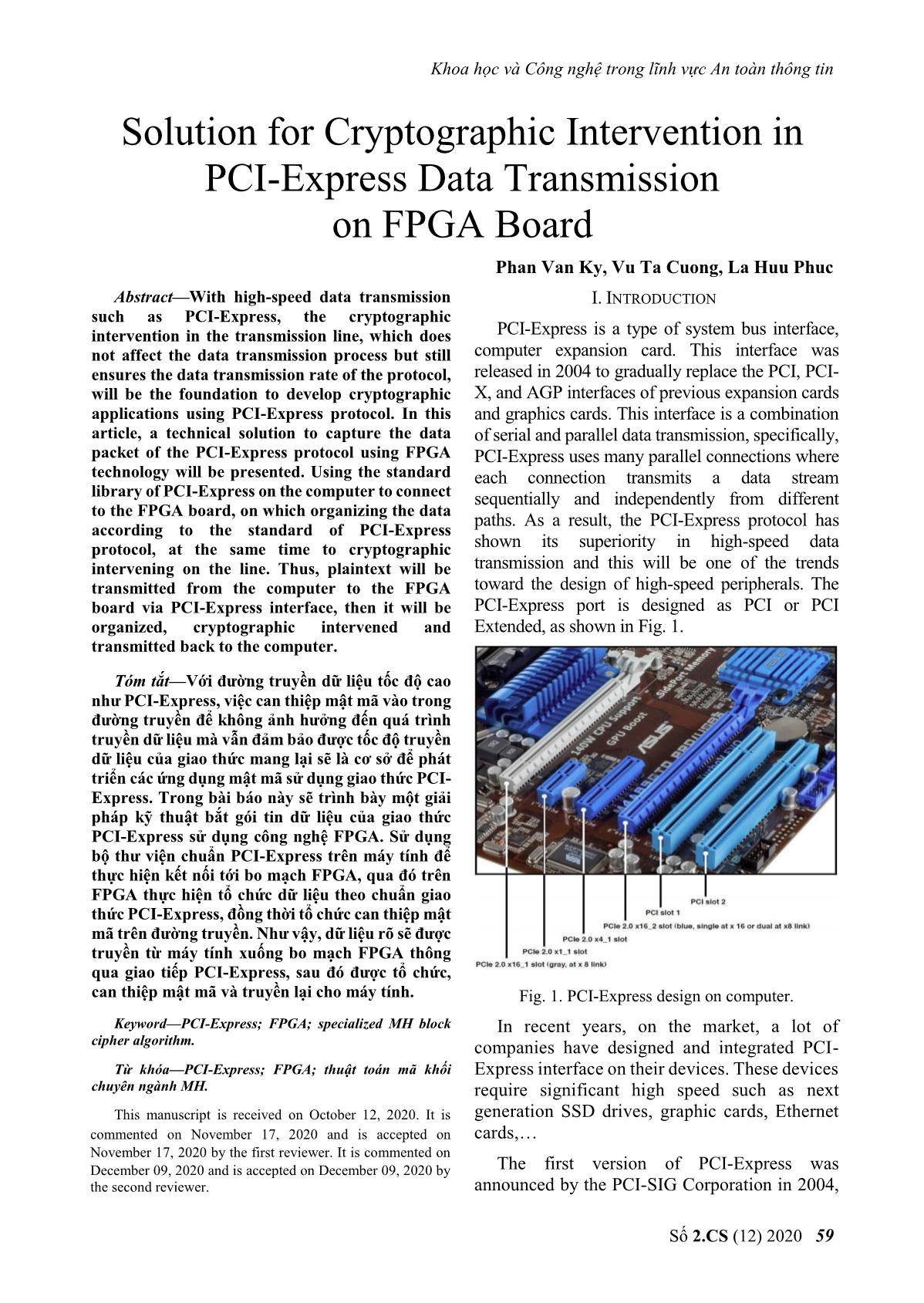
Trang 1
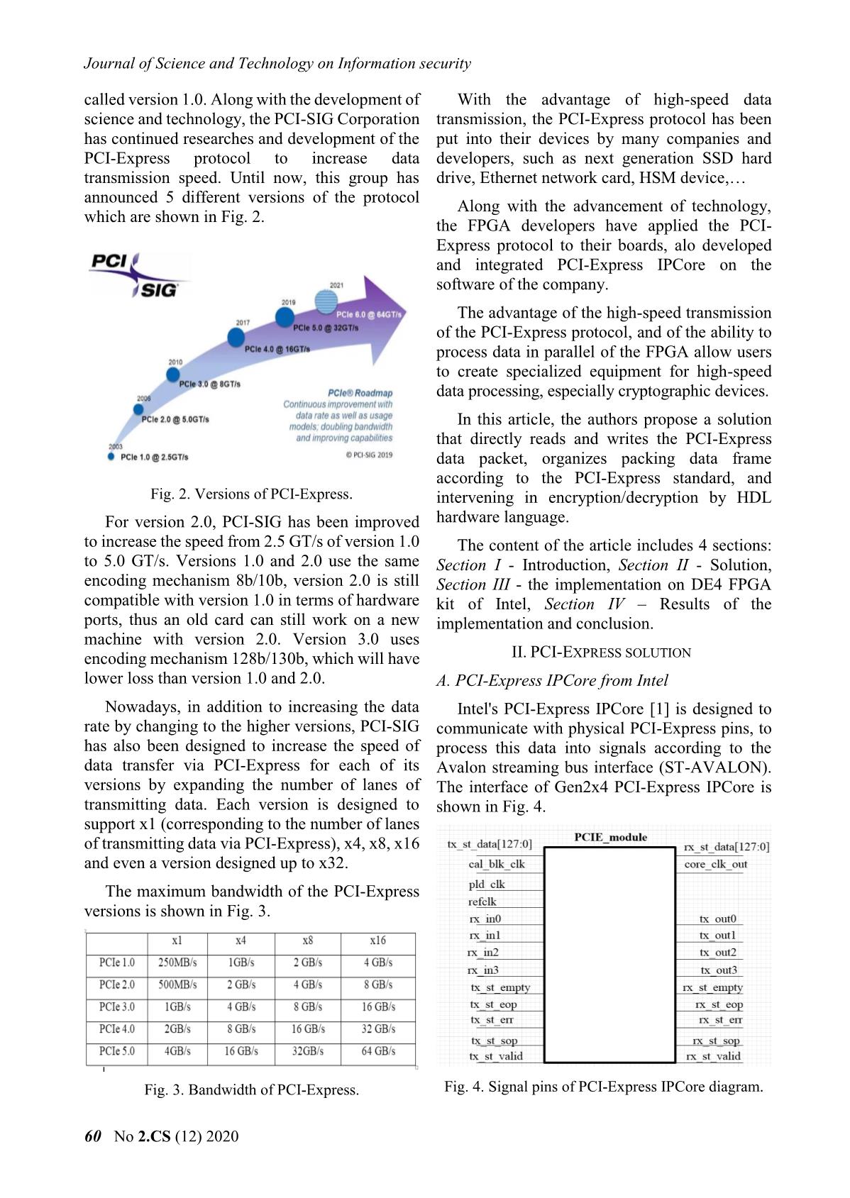
Trang 2
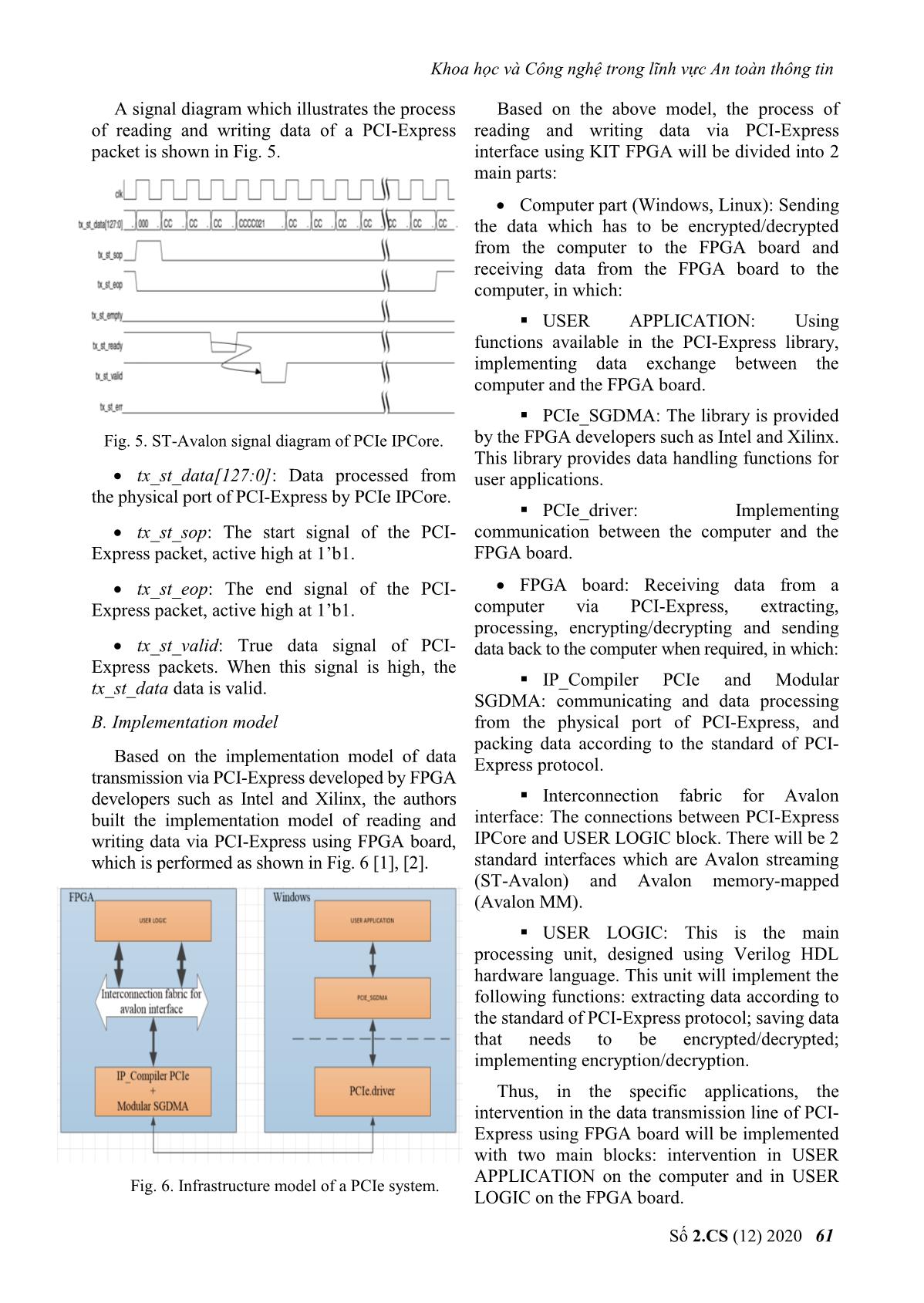
Trang 3
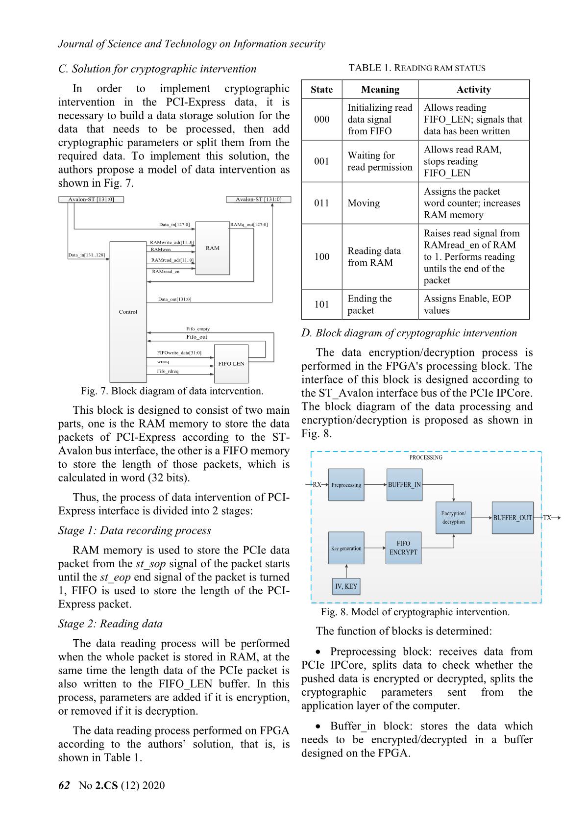
Trang 4
Trang 5
Trang 6
Trang 7
Trang 8
Trang 9

Trang 10
Tóm tắt nội dung tài liệu: Solution for Cryptographic Intervention in PCI-Express Data Transmission on FPGA Board
Khoa học và Công nghệ trong lĩnh vực An toàn thông tin
Số 2.CS (12) 2020 59
Solution for Cryptographic Intervention in
PCI-Express Data Transmission
on FPGA Board
Phan Van Ky, Vu Ta Cuong, La Huu Phuc
Abstract—With high-speed data transmission
such as PCI-Express, the cryptographic
intervention in the transmission line, which does
not affect the data transmission process but still
ensures the data transmission rate of the protocol,
will be the foundation to develop cryptographic
applications using PCI-Express protocol. In this
article, a technical solution to capture the data
packet of the PCI-Express protocol using FPGA
technology will be presented. Using the standard
library of PCI-Express on the computer to connect
to the FPGA board, on which organizing the data
according to the standard of PCI-Express
protocol, at the same time to cryptographic
intervening on the line. Thus, plaintext will be
transmitted from the computer to the FPGA
board via PCI-Express interface, then it will be
organized, cryptographic intervened and
transmitted back to the computer.
Tóm tắt—Với đường truyền dữ liệu tốc độ cao
như PCI-Express, việc can thiệp mật mã vào trong
đường truyền để không ảnh hưởng đến quá trình
truyền dữ liệu mà vẫn đảm bảo được tốc độ truyền
dữ liệu của giao thức mang lại sẽ là cơ sở để phát
triển các ứng dụng mật mã sử dụng giao thức PCI-
Express. Trong bài báo này sẽ trình bày một giải
pháp kỹ thuật bắt gói tin dữ liệu của giao thức
PCI-Express sử dụng công nghệ FPGA. Sử dụng
bộ thư viện chuẩn PCI-Express trên máy tính để
thực hiện kết nối tới bo mạch FPGA, qua đó trên
FPGA thực hiện tổ chức dữ liệu theo chuẩn giao
thức PCI-Express, đồng thời tổ chức can thiệp mật
mã trên đường truyền. Như vậy, dữ liệu rõ sẽ được
truyền từ máy tính xuống bo mạch FPGA thông
qua giao tiếp PCI-Express, sau đó được tổ chức,
can thiệp mật mã và truyền lại cho máy tính.
Keyword—PCI-Express; FPGA; specialized MH block
cipher algorithm.
Từ khóa—PCI-Express; FPGA; thuật toán mã khối
chuyên ngành MH.
This manuscript is received on October 12, 2020. It is
commented on November 17, 2020 and is accepted on
November 17, 2020 by the first reviewer. It is commented on
December 09, 2020 and is accepted on December 09, 2020 by
the second reviewer.
I. INTRODUCTION
PCI-Express is a type of system bus interface,
computer expansion card. This interface was
released in 2004 to gradually replace the PCI, PCI-
X, and AGP interfaces of previous expansion cards
and graphics cards. This interface is a combination
of serial and parallel data transmission, specifically,
PCI-Express uses many parallel connections where
each connection transmits a data stream
sequentially and independently from different
paths. As a result, the PCI-Express protocol has
shown its superiority in high-speed data
transmission and this will be one of the trends
toward the design of high-speed peripherals. The
PCI-Express port is designed as PCI or PCI
Extended, as shown in Fig. 1.
Fig. 1. PCI-Express design on computer.
In recent years, on the market, a lot of
companies have designed and integrated PCI-
Express interface on their devices. These devices
require significant high speed such as next
generation SSD drives, graphic cards, Ethernet
cards,
The first version of PCI-Express was
announced by the PCI-SIG Corporation in 2004,
Journal of Science and Technology on Information security
60 No 2.CS (12) 2020
called version 1.0. Along with the development of
science and technology, the PCI-SIG Corporation
has continued researches and development of the
PCI-Express protocol to increase data
transmission speed. Until now, this group has
announced 5 different versions of the protocol
which are shown in Fig. 2.
Fig. 2. Versions of PCI-Express.
For version 2.0, PCI-SIG has been improved
to increase the speed from 2.5 GT/s of version 1.0
to 5.0 GT/s. Versions 1.0 and 2.0 use the same
encoding mechanism 8b/10b, version 2.0 is still
compatible with version 1.0 in terms of hardware
ports, thus an old card can still work on a new
machine with version 2.0. Version 3.0 uses
encoding mechanism 128b/130b, which will have
lower loss than version 1.0 and 2.0.
Nowadays, in addition to increasing the data
rate by changing to the higher versions, PCI-SIG
has also been designed to increase the speed of
data transfer via PCI-Express for each of its
versions by expanding the number of lanes of
transmitting data. Each version is designed to
support x1 (corresponding to the number of lanes
of transmitting data via PCI-Express), x4, x8, x16
and even a version designed up to x32.
The maximum bandwidth of the PCI-Express
versions is shown in Fig. 3.
Fig. 3. Bandwidth of PCI-Express.
With the advantage of high-speed data
transmission, the PCI-Express protocol has been
put into their devices by many companies and
developers, such as next generation SSD hard
drive, Ethernet network card, HSM device,
Along with the advancement of technology,
the FPGA developers have applied the PCI-
Express protocol to their boards, alo developed
and integrated PCI-Express IPCore on the
software of the company.
The advantage of the high-speed transmission
of the PCI-Express protocol, and of the ability to
process data in parallel of the FPGA allow users
to create specialized equipment for high-speed
data processing, especially cryptographic devices.
In this article, the authors propose a solution
that directly reads and writes the PCI-Express
data packet, organizes packing data frame
according to the PCI-Express standard, and
intervening in encryption/decryption by HDL
hardware language.
The content of the article includes 4 sections:
Section I - Introduction, Section II - Solution,
Section III - the implementation on DE4 FPGA
kit of Intel, Section IV ... pted/decrypted. This data will be
stored in the memory on the FPGA. And during
writing data to the FPGA, the key generation
block will take the IV and the current key to
generate the stream keys and store it in a buffer,
in order to require the data transmission line of the
PCI-Express. When there is a reading signal, the
encrypted/decrypted data will be sent to
the computer.
E. Design of key generation block on FPGA
In this article, the authors use the specialized
MH cipher algorithm to perform the
cryptographic intervention in the transmission
line of PCI-Express. Thus, on the FPGA board,
MH cipher algorithm is designed as follows and
in Fig. 9:
 Data input: 128 bits
 Key: 256 bits.
 Working clock: 125 MHz, according to the
working frequency of PCI-Express IPCore.
 Data output: 128 bits.
MH
Key
Data_in[127:0]
start
Data_out[127:0]
Done
Fig. 9. Signal pin diagram of MH core.
Design of the Key generation block, depends on
the problem and different modes. In this article, the
authors mainly focus on the problem of examining
the feasibility of the cryptographic intervention in
the data transmission line of PCI-Express.
Therefore, the authors design the Key generation
block in CTR mode and use many MH cores to
speed up the encryption/decryption. The solution
for Key generation block is shown in Fig. 10.
MH_26core FIFO_ENCRYPT
Key extension
IV
VXL
KEY
Key_out
127:0
127:0 127:0
Fig. 10. Key generation model
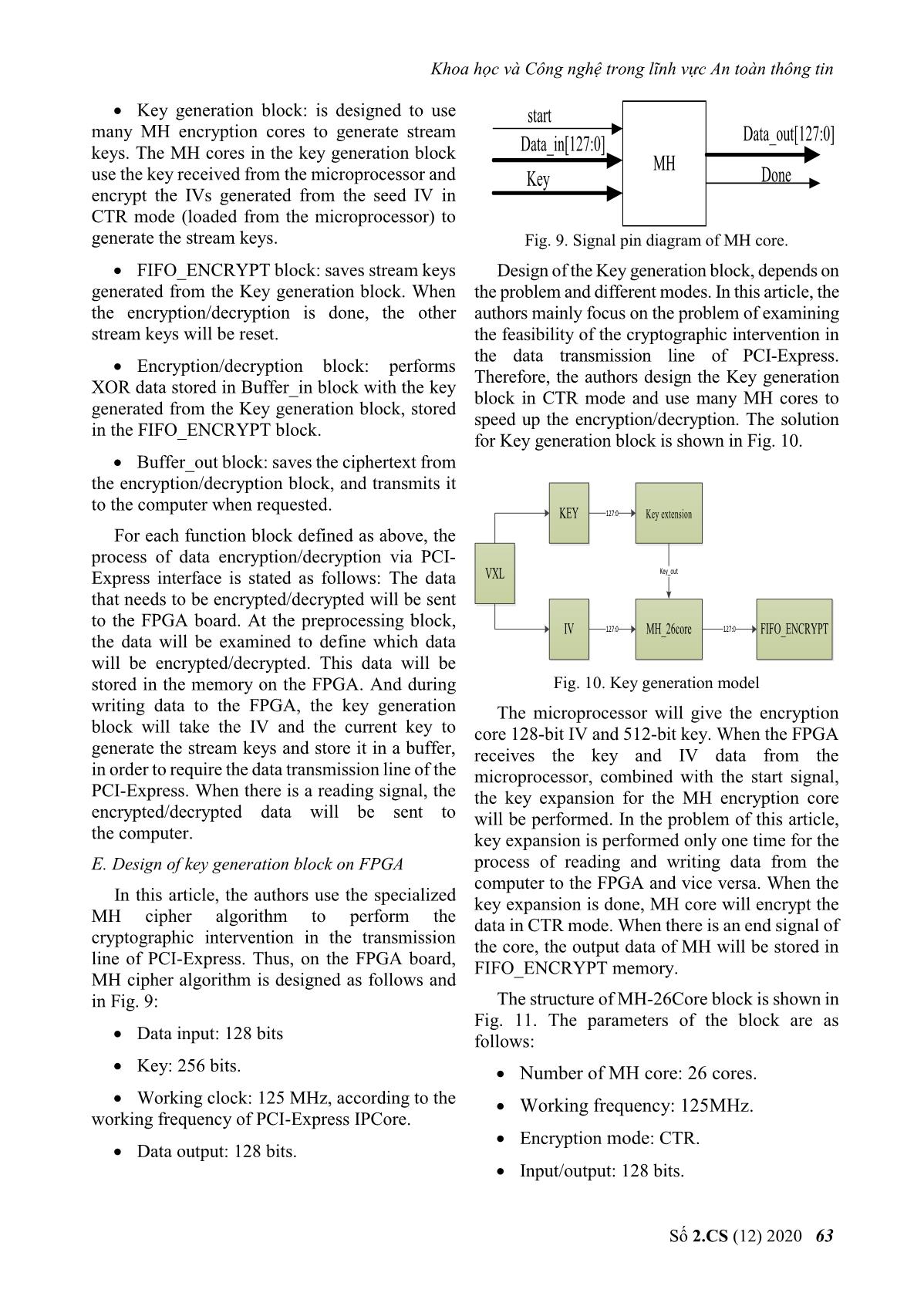
The microprocessor will give the encryption
core 128-bit IV and 512-bit key. When the FPGA
receives the key and IV data from the
microprocessor, combined with the start signal,
the key expansion for the MH encryption core
will be performed. In the problem of this article,
key expansion is performed only one time for the
process of reading and writing data from the
computer to the FPGA and vice versa. When the
key expansion is done, MH core will encrypt the
data in CTR mode. When there is an end signal of
the core, the output data of MH will be stored in
FIFO_ENCRYPT memory.
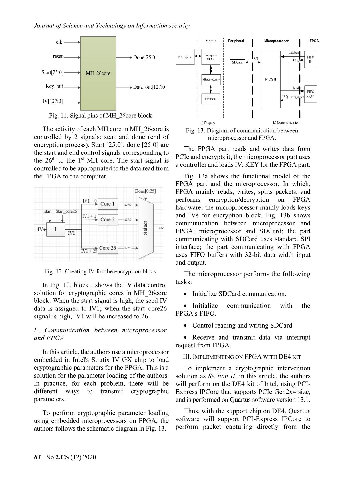
The structure of MH-26Core block is shown in
Fig. 11. The parameters of the block are as
follows:
 Number of MH core: 26 cores.
 Working frequency: 125MHz.
 Encryption mode: CTR.
 Input/output: 128 bits.
Journal of Science and Technology on Information security
64 No 2.CS (12) 2020
MH_26core
clk
reset
Start[25:0]
Key_out
IV[127:0]
Done[25:0]
Data_out[127:0]
Fig. 11. Signal pins of MH_26core block
The activity of each MH core in MH_26core is
controlled by 2 signals: start and done (end of
encryption process). Start [25:0], done [25:0] are
the start and end control signals corresponding to
the 26th to the 1st MH core. The start signal is
controlled to be appropriated to the data read from
the FPGA to the computer.
Fig. 12. Creating IV for the encryption block
In Fig. 12, block I shows the IV data control
solution for cryptographic cores in MH_26core
block. When the start signal is high, the seed IV
data is assigned to IV1; when the start_core26
signal is high, IV1 will be increased to 26.
F. Communication between microprocessor
and FPGA
In this article, the authors use a microprocessor
embedded in Intel's Stratix IV GX chip to load
cryptographic parameters for the FPGA. This is a
solution for the parameter loading of the authors.
In practice, for each problem, there will be
different ways to transmit cryptographic
parameters.
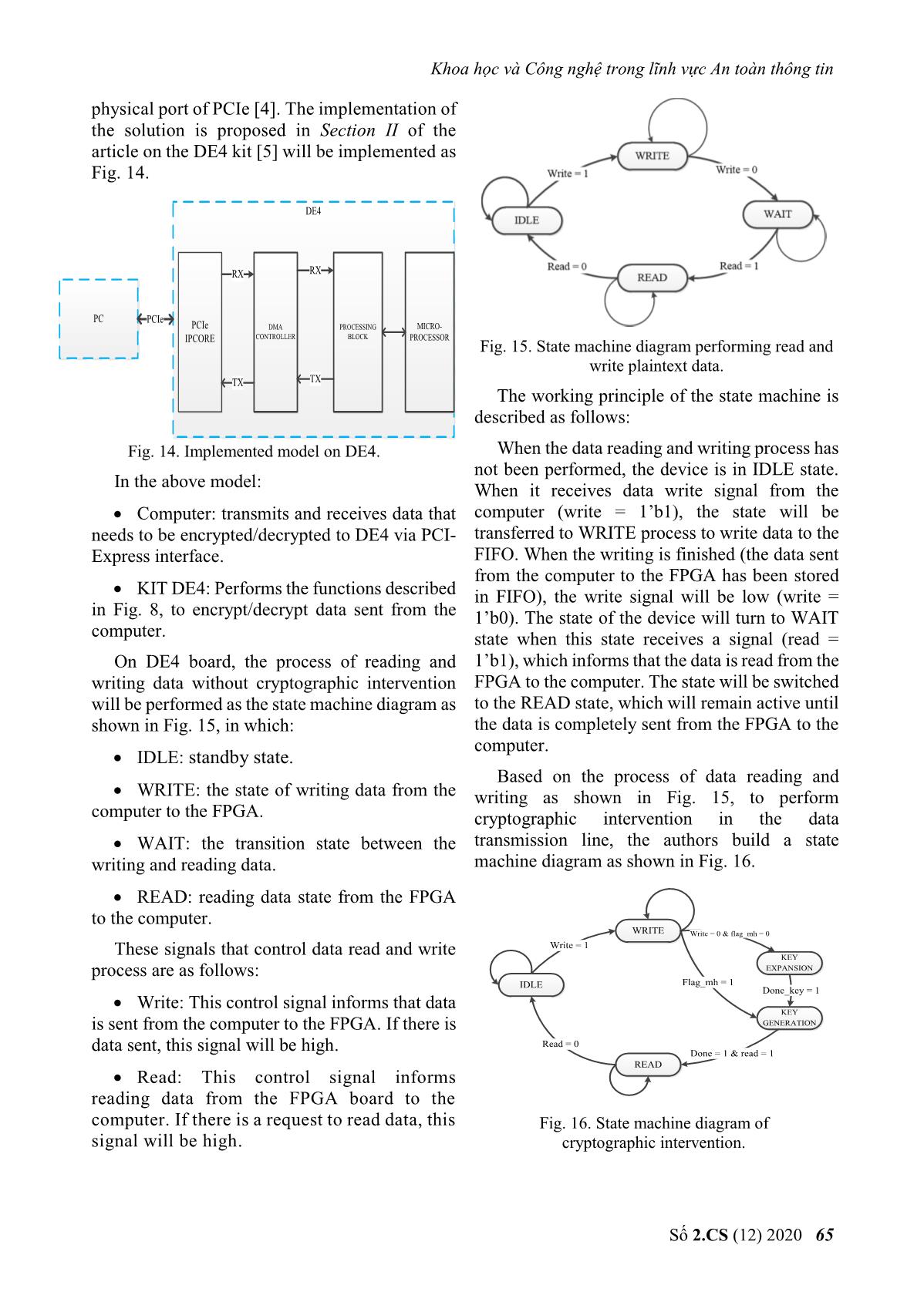
To perform cryptographic parameter loading
using embedded microprocessors on FPGA, the
authors follows the schematic diagram in Fig. 13.
PCI-Express
Encryption
(HDL)
Microprocessor
Peripheral
Statrix IV
NIOS II
SPI
SDCard
FIFO
IN
FIFO
OUT
databus
databus
IRQ
Fifo_full
Fifo_empty
MicroprocessorPeripheral FPGA
a) Diagram b) Communication
Fig. 13. Diagram of communication between
microprocessor and FPGA.
The FPGA part reads and writes data from
PCIe and encrypts it; the microprocessor part uses
a controller and loads IV, KEY for the FPGA part.
Fig. 13a shows the functional model of the
FPGA part and the microprocessor. In which,
FPGA mainly reads, writes, splits packets, and
performs encryption/decryption on FPGA
hardware; the microprocessor mainly loads keys
and IVs for encryption block. Fig. 13b shows
communication between microprocessor and
FPGA; microprocessor and SDCard; the part
communicating with SDCard uses standard SPI
interface; the part communicating with FPGA
uses FIFO buffers with 32-bit data width input
and output.
The microprocessor performs the following
tasks:
 Initialize SDCard communication.
 Initialize communication with the
FPGA's FIFO.
 Control reading and writing SDCard.
 Receive and transmit data via interrupt
request from FPGA.
III. IMPLEMENTING ON FPGA WITH DE4 KIT
To implement a cryptographic intervention
solution as Section II, in this article, the authors
will perform on the DE4 kit of Intel, using PCI-
Express IPCore that supports PCIe Gen2x4 size,
and is performed on Quartus software version 13.1.
Thus, with the support chip on DE4, Quartus
software will support PCI-Express IPCore to
perform packet capturing directly from the
Khoa học và Công nghệ trong lĩnh vực An toàn thông tin
Số 2.CS (12) 2020 65
physical port of PCIe [4]. The implementation of
the solution is proposed in Section II of the
article on the DE4 kit [5] will be implemented as
Fig. 14.
DE4
PC PCIe
PCIe
IPCORE
DMA
CONTROLLER
RX
TX
PROCESSING
BLOCK
RX
TX
MICRO-
PROCESSOR
Fig. 14. Implemented model on DE4.
In the above model:
 Computer: transmits and receives data that
needs to be encrypted/decrypted to DE4 via PCI-
Express interface.
 KIT DE4: Performs the functions described
in Fig. 8, to encrypt/decrypt data sent from the
computer.
On DE4 board, the process of reading and
writing data without cryptographic intervention
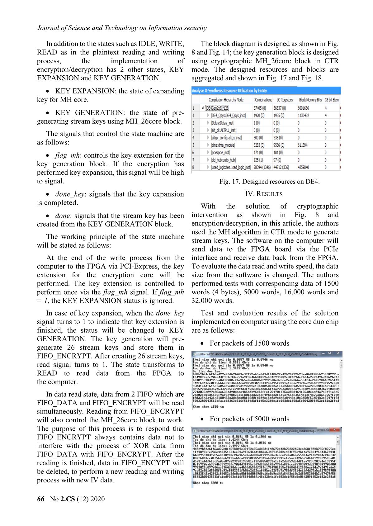
will be performed as the state machine diagram as
shown in Fig. 15, in which:
 IDLE: standby state.
 WRITE: the state of writing data from the
computer to the FPGA.
 WAIT: the transition state between the
writing and reading data.
 READ: reading data state from the FPGA
to the computer.
These signals that control data read and write
process are as follows:
 Write: This control signal informs that data
is sent from the computer to the FPGA. If there is
data sent, this signal will be high.
 Read: This control signal informs
reading data from the FPGA board to the
computer. If there is a request to read data, this
signal will be high.
Fig. 15. State machine diagram performing read and
write plaintext data.
The working principle of the state machine is
described as follows:
When the data reading and writing process has
not been performed, the device is in IDLE state.
When it receives data write signal from the
computer (write = 1’b1), the state will be
transferred to WRITE process to write data to the
FIFO. When the writing is finished (the data sent
from the computer to the FPGA has been stored
in FIFO), the write signal will be low (write =
1’b0). The state of the device will turn to WAIT
state when this state receives a signal (read =
1’b1), which informs that the data is read from the
FPGA to the computer. The state will be switched
to the READ state, which will remain active until
the data is completely sent from the FPGA to the
computer.
Based on the process of data reading and
writing as shown in Fig. 15, to perform
cryptographic intervention in the data
transmission line, the authors build a state
machine diagram as shown in Fig. 16.
IDLE
WRITE
KEY
EXPANSION
READ
KEY
GENERATION
Write = 1
Write = 0 & flag_mh = 0
Done_key = 1
Done = 1 & read = 1
Read = 0
Flag_mh = 1
Fig. 16. State machine diagram of
cryptographic intervention.
Journal of Science and Technology on Information security
66 No 2.CS (12) 2020
In addition to the states such as IDLE, WRITE,
READ as in the plaintext reading and writing
process, the implementation of
encryption/decryption has 2 other states, KEY
EXPANSION and KEY GENERATION.
 KEY EXPANSION: the state of expanding
key for MH core.
 KEY GENERATION: the state of pre-
generating stream keys using MH_26core block.
The signals that control the state machine are
as follows:
 flag_mh: controls the key extension for the
key generation block. If the encryption has
performed key expansion, this signal will be high
to signal.
 done_key: signals that the key expansion
is completed.
 done: signals that the stream key has been
created from the KEY GENERATION block.
The working principle of the state machine
will be stated as follows:
At the end of the write process from the
computer to the FPGA via PCI-Express, the key
extension for the encryption core will be
performed. The key extension is controlled to
perform once via the flag_mh signal. If flag_mh
= 1, the KEY EXPANSION status is ignored.
In case of key expansion, when the done_key
signal turns to 1 to indicate that key extension is
finished, the status will be changed to KEY
GENERATION. The key generation will pre-
generate 26 stream keys and store them in
FIFO_ENCRYPT. After creating 26 stream keys,
read signal turns to 1. The state transforms to
READ to read data from the FPGA to
the computer.
In data read state, data from 2 FIFO which are
FIFO_DATA and FIFO_ENCRYPT will be read
simultaneously. Reading from FIFO_ENCRYPT
will also control the MH_26core block to work.
The purpose of this process is to respond that
FIFO_ENCRYPT always contains data not to
interfere with the process of XOR data from
FIFO_DATA with FIFO_ENCRYPT. After the
reading is finished, data in FIFO_ENCYPT will
be deleted, to perform a new reading and writing
process with new IV data.
The block diagram is designed as shown in Fig.
8 and Fig. 14; the key generation block is designed
using cryptographic MH_26core block in CTR
mode. The designed resources and blocks are
aggregated and shown in Fig. 17 and Fig. 18.
Fig. 17. Designed resources on DE4.
IV. RESULTS
With the solution of cryptographic
intervention as shown in Fig. 8 and
encryption/decryption, in this article, the authors
used the MH algorithm in CTR mode to generate
stream keys. The software on the computer will
send data to the FPGA board via the PCIe
interface and receive data back from the FPGA.
To evaluate the data read and write speed, the data
size from the software is changed. The authors
performed tests with corresponding data of 1500
words (4 bytes), 5000 words, 16,000 words and
32,000 words.
Test and evaluation results of the solution
implemented on computer using the core duo chip
are as follows:
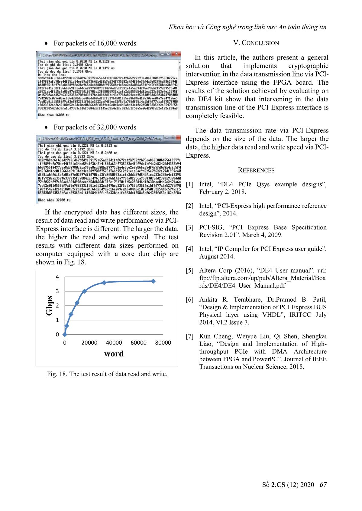
 For packets of 1500 words
 For packets of 5000 words
Khoa học và Công nghệ trong lĩnh vực An toàn thông tin
Số 2.CS (12) 2020 67
 For packets of 16,000 words
 For packets of 32,000 words
If the encrypted data has different sizes, the
result of data read and write performance via PCI-
Express interface is different. The larger the data,
the higher the read and write speed. The test
results with different data sizes performed on
computer equipped with a core duo chip are
shown in Fig. 18.
Fig. 18. The test result of data read and write.
V. CONCLUSION
In this article, the authors present a general
solution that implements cryptographic
intervention in the data transmission line via PCI-
Express interface using the FPGA board. The
results of the solution achieved by evaluating on
the DE4 kit show that intervening in the data
transmission line of the PCI-Express interface is
completely feasible.
The data transmission rate via PCI-Express
depends on the size of the data. The larger the
data, the higher data read and write speed via PCI-
Express.
REFERENCES
[1] Intel, “DE4 PCIe Qsys example designs”,
February 2, 2018.
[2] Intel, “PCI-Express high performance reference
design”, 2014.
[3] PCI-SIG, “PCI Express Base Specification
Revision 2.01”, March 4, 2009.
[4] Intel, “IP Compiler for PCI Express user guide”,
August 2014.
[5] Altera Corp (2016), “DE4 User manual”. url:
ftp://ftp.altera.com/up/pub/Altera_Material/Boa
rds/DE4/DE4_User_Manual.pdf
[6] Ankita R. Tembhare, Dr.Pramod B. Patil,
“Design & Implementation of PCI Express BUS
Physical layer using VHDL”, IRITCC July
2014, Vl.2 Issue 7.
[7] Kun Cheng, Weiyue Liu, Qi Shen, Shengkai
Liao, “Design and Implementation of High-
throughput PCIe with DMA Architecture
between FPGA and PowerPC”, Journal of IEEE
Transactions on Nuclear Science, 2018.
0
1
2
3
4
0 20000 40000 60000 80000
G
b
p
s
word
Journal of Science and Technology on Information security
68 No 2.CS (12) 2020
ABOUT THE AUTHOR
Phan Van Ky
Workplace: Institute of Cryptographic
Science and Technology
Email: pvk.hvktqs@gmail.com
Education: Received bachelor’s degree
in 2013, received master’s degree in
2017, in Saint Petersburg Electronical
University.
Current research field: integrated circuit technology, FPGA.
Vu Ta Cuong
Workplace: Institute of
Cryptographic Science and
Technology
Email: vutacuong109@gmail.com
Education: Received bachelor's
degree in 2011, master's degree in
2013, and PhD in 2016, in Radio Electronics, Kharkiv
Aerospace University, Ukraine.
Current research field: PKI Token, cryptographic
engineering.
La Huu Phuc
Workplace: Institute of
Cryptographic Science and
Technology
Email: phucpvkt@hotmail.com
Education: Received bachelor's degree
in 1998, master’s degree in 2002, and
PhD in 2015 in Electronic engineering.
Current research field: Designing and producing security
device, specialized cipher machine.
File đính kèm:
 solution_for_cryptographic_intervention_in_pci_express_data.pdf

